User booking system
Myfab LIMS
Tool List
Pictures and specifications of our equipment can be found here.
Technologies
Electron Beam Lithography
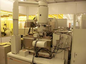
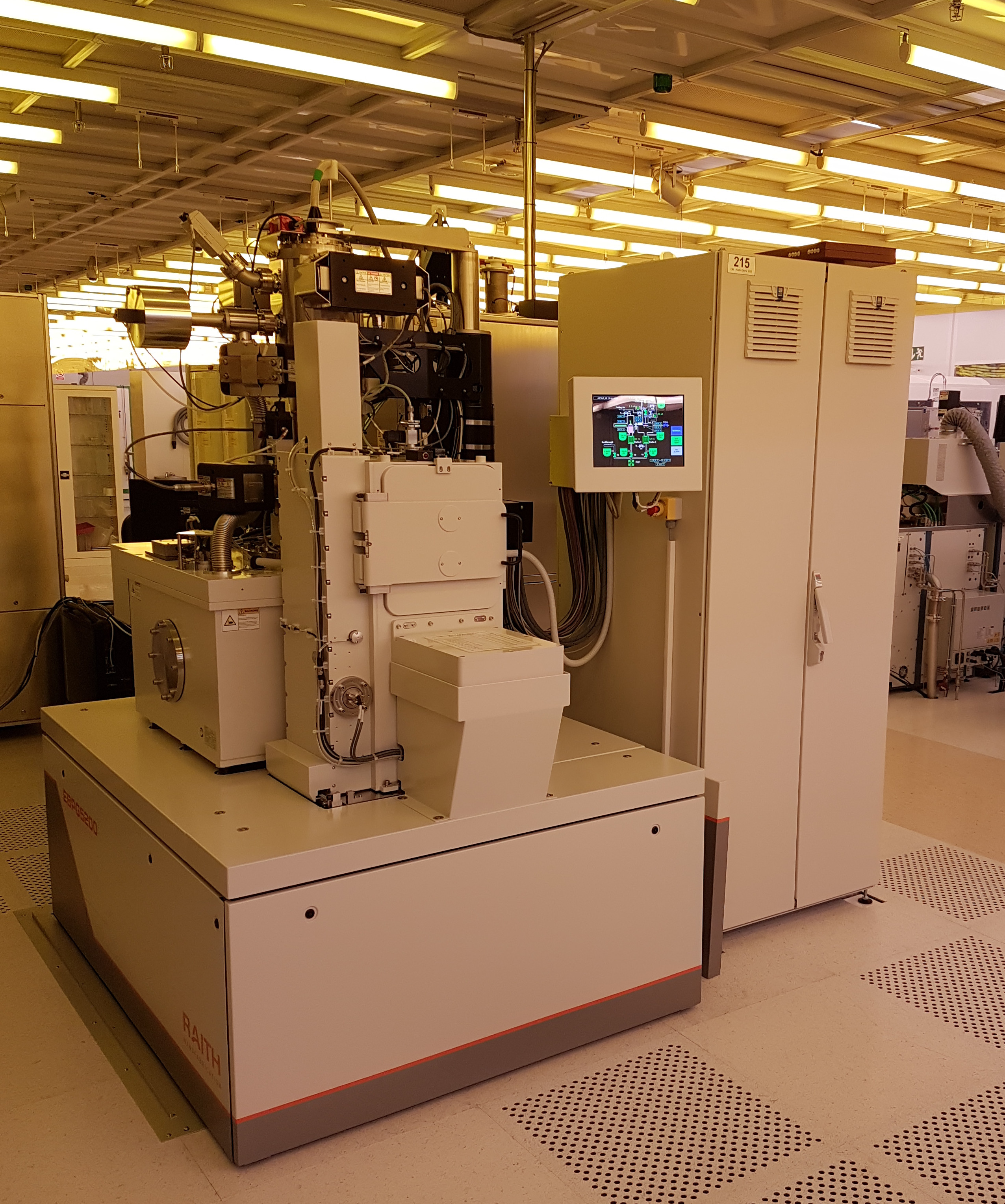
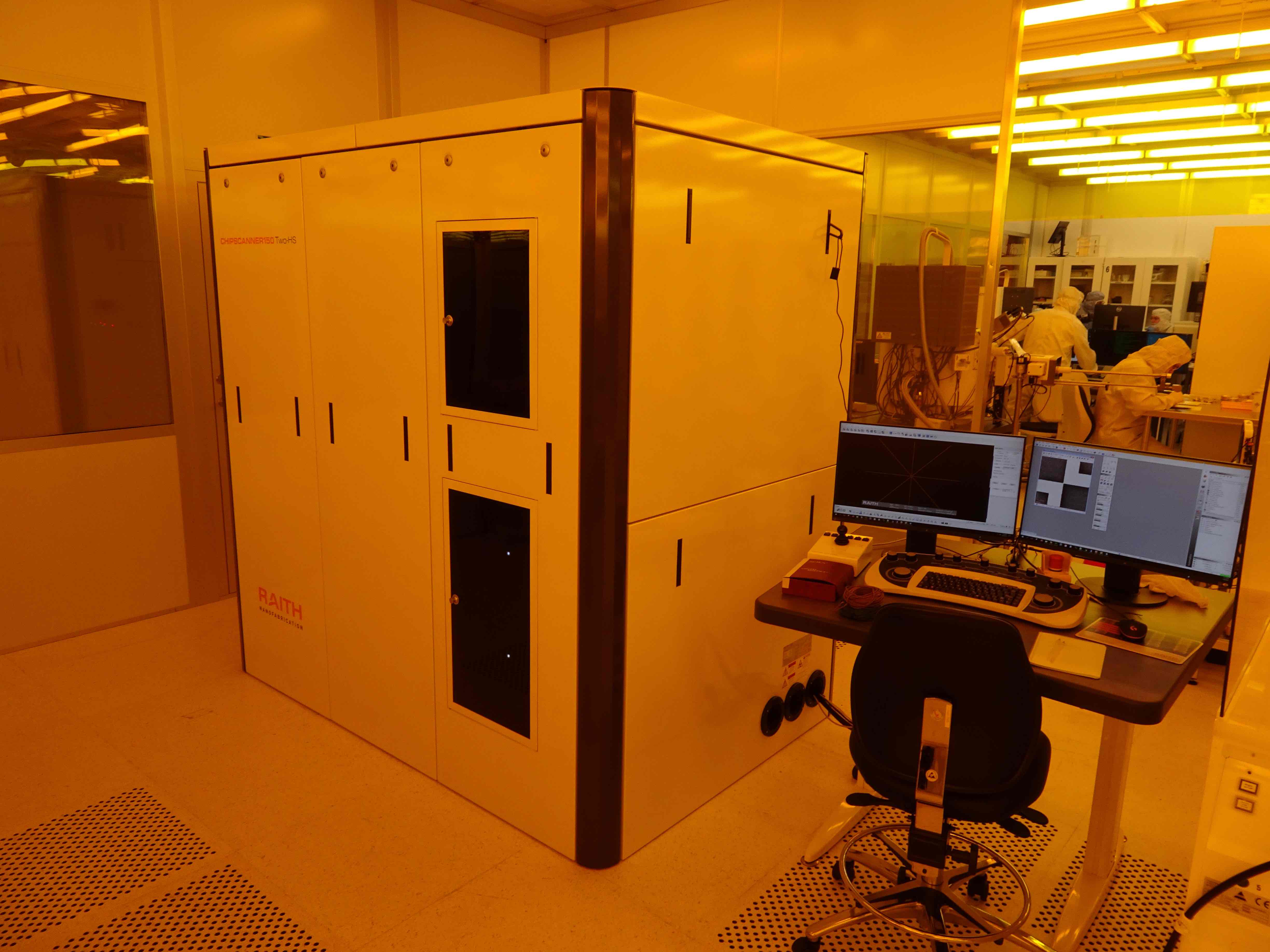
Myfab Chalmers has a very long tradition of nanolithography. We have two high end systems in operation, a JEOL 9300FS and a Raith EPBG 5200 and three staff dedicated to this technology. We also have a Raith chip scanner 150TWO-HS for automated SEM imageing.
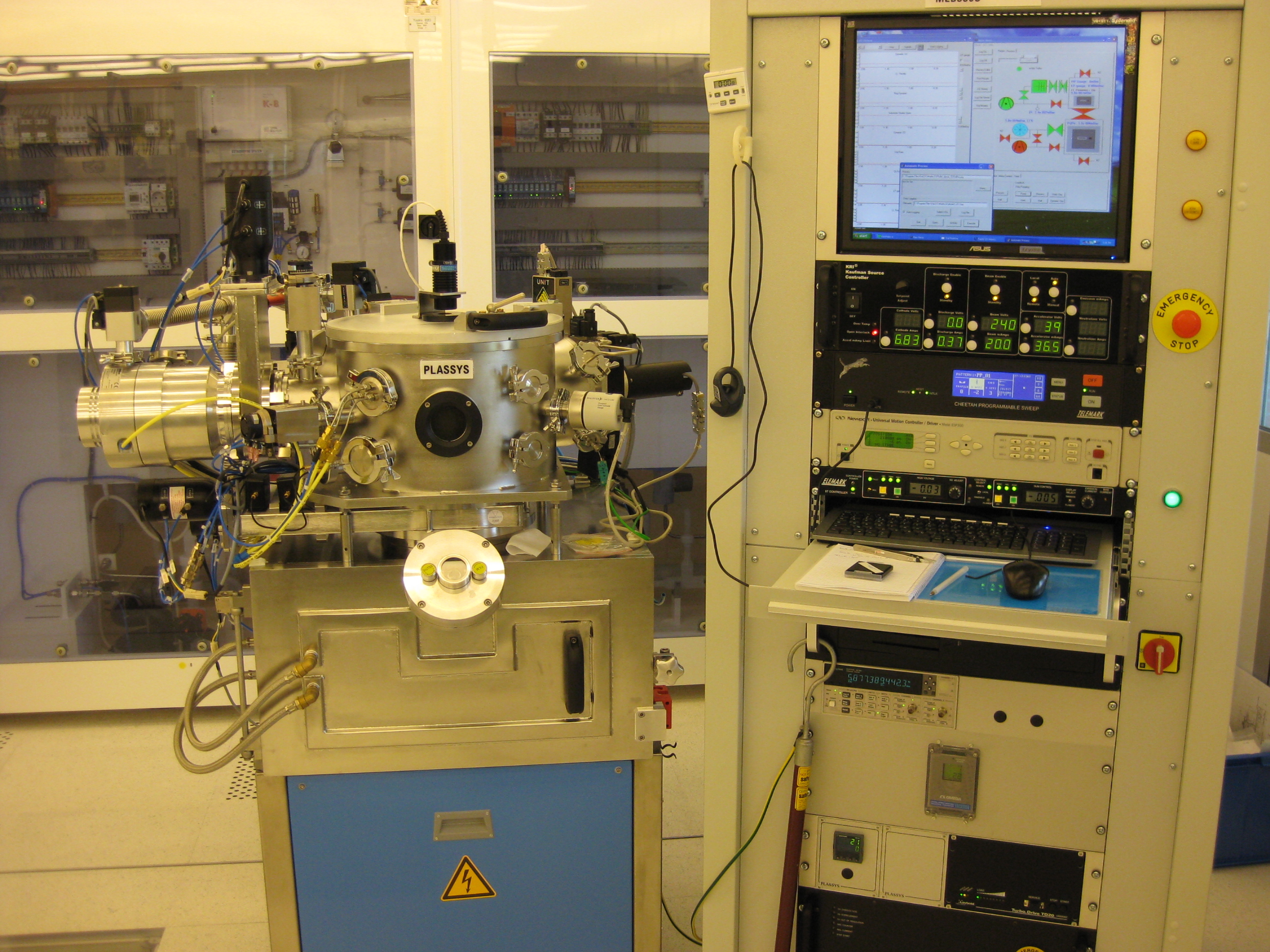
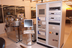
Thin Film Deposition
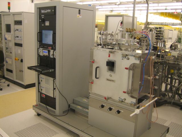
A wide variety of metal and insulating thin films can be deposited by a number of evaporation and sputter systems.
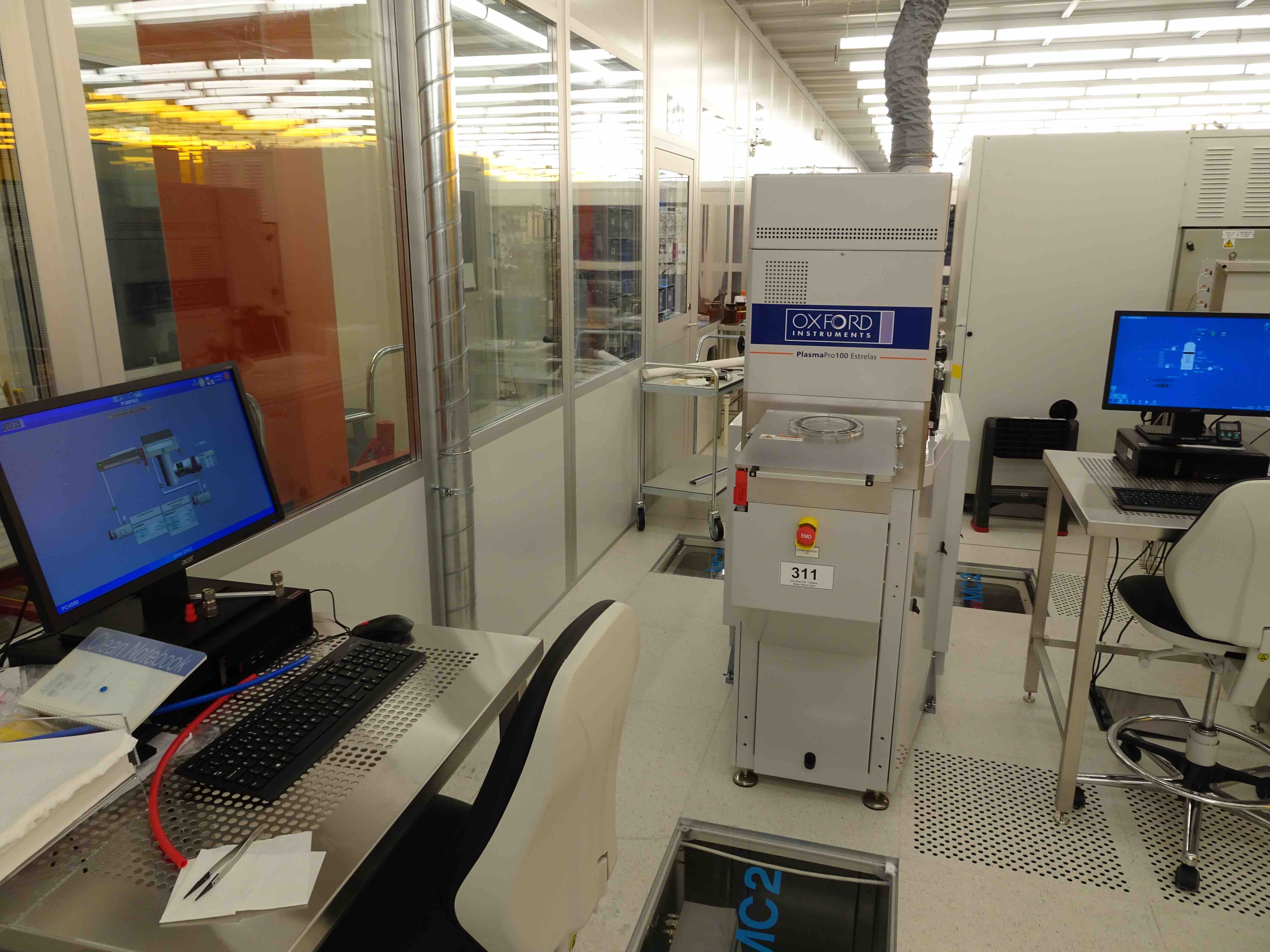
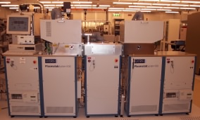
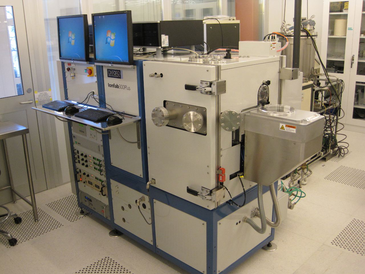
Plasma Processing
The Laboratory has a wide assortment of plasma tools for dry etching and deposition.
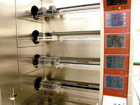
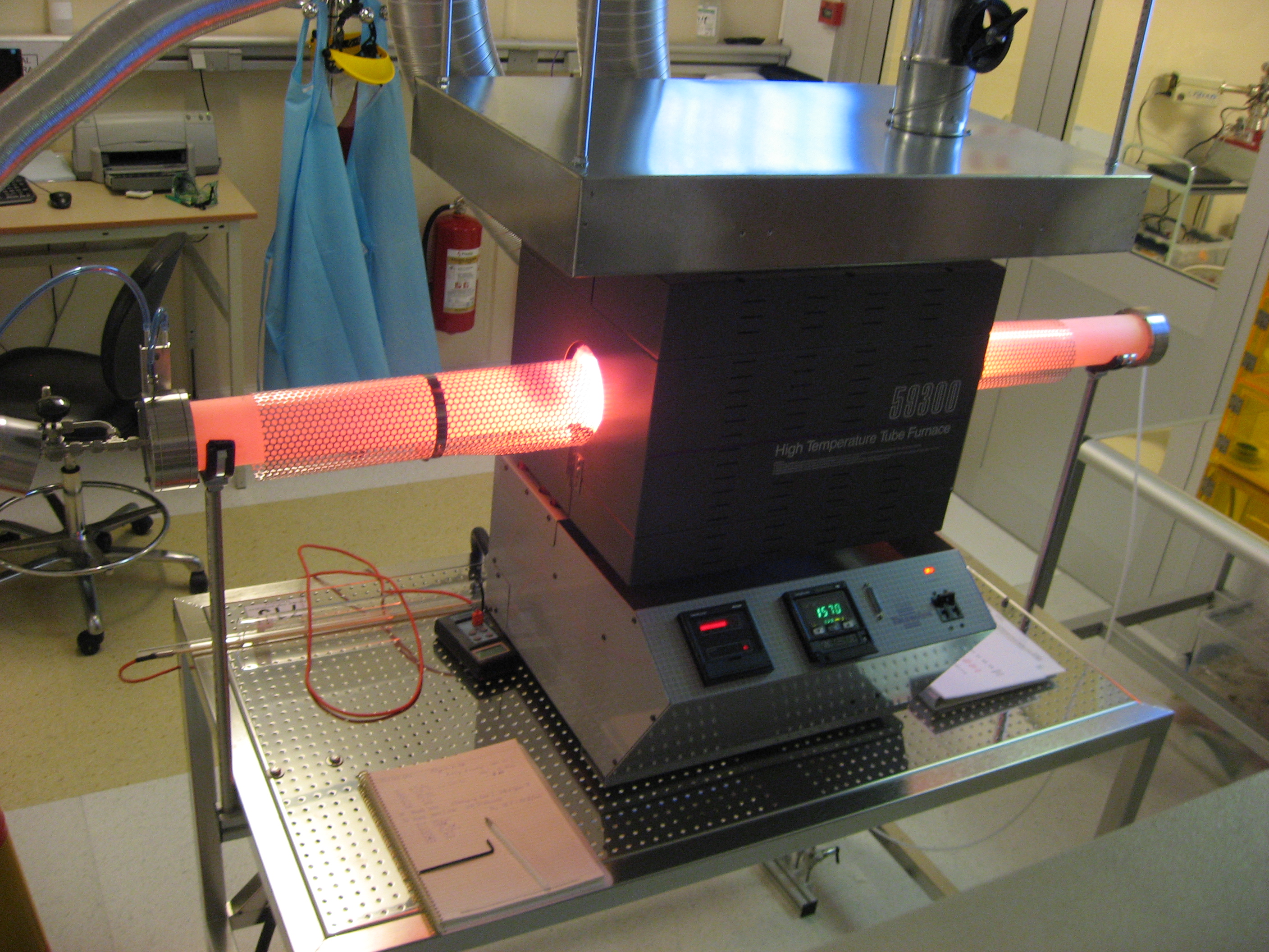
Thermal Processing
Chalmers has the ability to thermally process Si wafers up to 150 mm in diameter in its 4 four-stack Centrotherm E2000 furnaces capable of LPCVD, oxidation, and annealing.
Processing Lines
Microwave & Photonic Processing Line
The microwave and photonic processing line consists of a complete set of process tools for the fabrication of microwave and photonic devices and components. Process tools which make up the line are either strictly limited to microwave/photonic devices, or have a limited number of approved processes which have been demonstrated to not have any adverse effects on microwave/photonic processing. The line has resulted in improved stability, quality, and yield in the complicated process flows used in wide bandgap, low-noise, photonic, and terahertz devices. These are finding use in, for example, space applications for projects run through the European Space Agency. The materials processed on this line are predominantly SiC, GaN, and InP based MMICs as well as GaAs based VCSELs.
Nano & Quantum Technology Line
The nano & quantum technology line serves to increase the Laboratory’s ability to produce state-of-the-art superconducting and quantum devices and novel nano components in higher yield. The line is anchored around Chalmers’ long history and competence within electron beam lithography. Particular focus is being laid on attaining high yield on structures smaller than 20nm. With research and development in nanotechnology booming, this process line positions Chalmers to continue to be innovative for years to come. A very broad range of applications is served by this line, from bioelectronics to single electron devices.