Skip to content

Electric field doubles the speed of ultrafast magnetic processes

Schematic of a graphene spin field-effect junction, where ultrafast spin dynamics are captured using a femtosecond pump (red arrow)–probe (purple arrow) technique. Image: David Muradas-Belinchón and Venkata Mutta.

Researchers at Uppsala University, have together with international collaborators, developed a new device that speeds up magnetic processes using only an electric field, without the need to alter the shape or material. The results could enable faster data processing and memory storage for energy-efficient AI, and potentially facilitate new quantum technologies.

Modern electronic devices work by controlling the flow of electric current, that is the movement of electrons. However, electrons, in addition to their negative charge, also possess a magnetic property called spin, which is like a tiny magnet. In fact, these tiny electronic magnets together make a material magnetic. Combining electronics with magnetism has given rise to the field of spintronics, which uses the spin of electrons and has enabled groundbreaking advancements in data storage capacity in hard disk drives and got much smaller and much more effecient, from refrigerator-sized disk drives with a few MB memory storage capacity to coin-sized disk drives with TB memory storage capacity.

Increasing the speed of data storage can be transformational for reducing power consumption in data centres, such as Google Drive or BOX, and artificial intelligence infrastructure, like ChatGPT. This requires magnets to switch faster, and the challenge is to achieve this without altering the magnetic material or shape in devices.

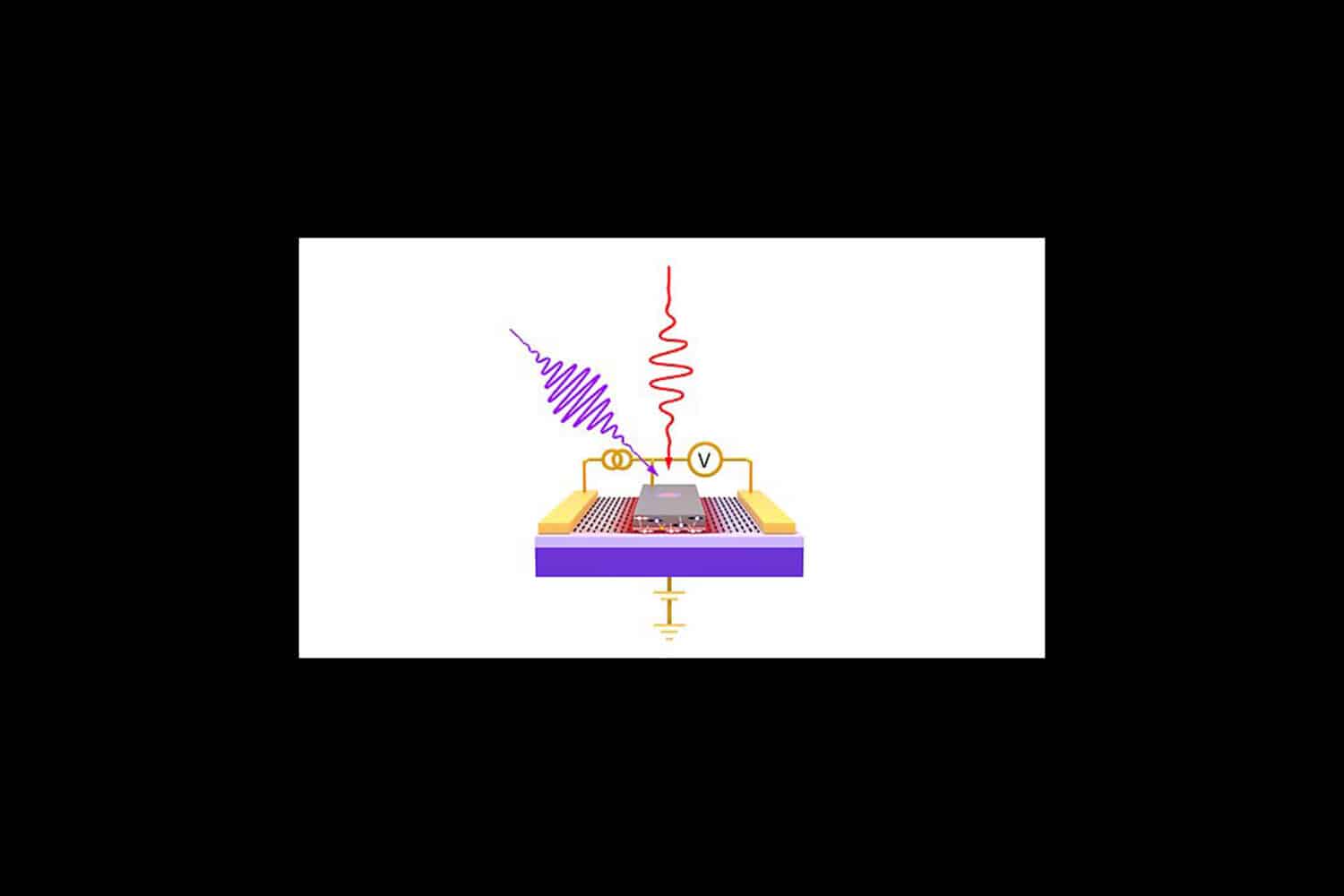
For the first time, researchers have developed a new device called a spin field effect junction, SFEJ, that can double the speed of demagnetization of a magnetic thin film by an electric field.

Highlights and events

Ove Öhman has been a bridge-builder between academia and the business sector for several decades and has helped strengthen Uppsala’s innovation environment. Photo: Mikael Wallerstedt, Uppsala University
2026 03 10
Myfab Uppsala

Ove Öhman receives prize as a bridge-builder between research and innovation

Read more
A research team at Chalmers University of Technology has developed a new diminutive laser technology that makes it possible to create a miniature biosensor with the laser source and optics integrated onto a one-centimetre semiconductor chip. This enables significantly smaller sensors, paving the way for portable optical technology and for moving certain types of medical sampling from hospitals to the patients’ homes. Illustration: Chalmers/Erik Strandberg
2026 03 10
Myfab Chalmers

Miniature laser technology could bring lab testing into your home

Read more
Event a university house - Ångström Laboratory - Myfab Uppsala
2026 02 25
Myfab Chalmers , Myfab , Myfab KTH , Myfab Lund , Myfab Uppsala

Register latest March 15: NNTN & NNUM in Uppsala

Read more
2026 02 24
Myfab KTH

KISAB speeds development of key clean‑energy materials with Myfab KTH’s support

Read more
See all highlights