
Highlights
2026 06 15
Myfab
,
Myfab Chalmers
,
Myfab KTH
,
Myfab Lund
,
Myfab Uppsala
Several researchers active within Myfab awarded associate senior lecturer grants
Read more
2026 06 15
Myfab Chalmers
,
Myfab
Simone Gasparinetti awarded Nagel Prize in Physics, by KVA
Read more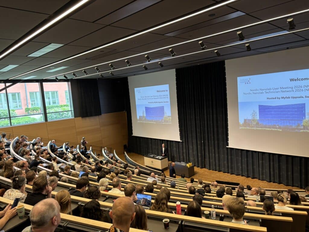
2026 06 03
Myfab
,
Myfab Chalmers
,
Myfab KTH
,
Myfab Lund
,
Myfab Uppsala
Nordic Nanolab meeting reaches record-high attendance
Read more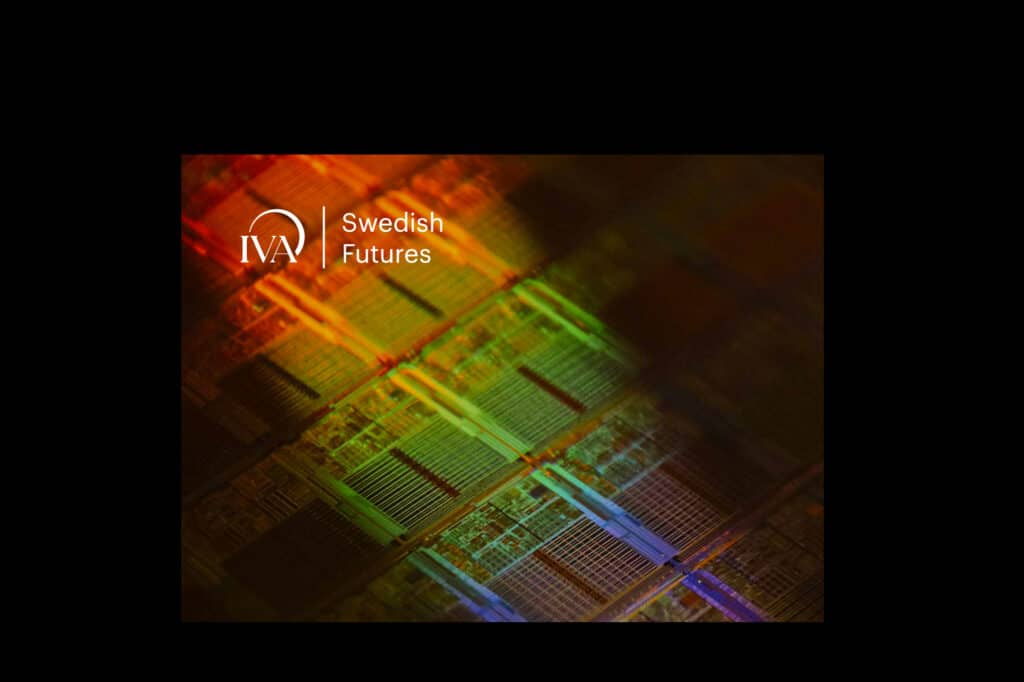
2026 05 27
Myfab
,
Myfab Chalmers
,
Myfab KTH
,
Myfab Lund
,
Myfab Uppsala
New report highlights the need to strengthen Sweden’s semiconductor ecosystem
Read more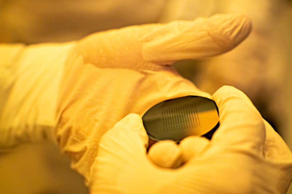
2026 05 12
Myfab
,
Myfab Chalmers
,
Myfab KTH
,
Myfab Lund
,
Myfab Uppsala
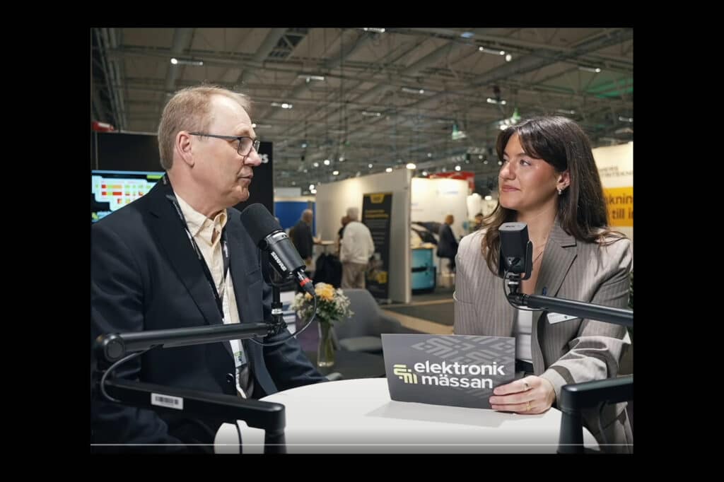
Excellence cluster applications – Myfab plays a key role
Read more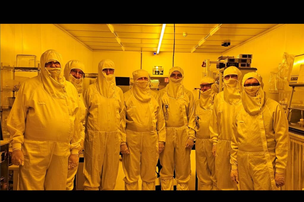
2026 05 04
Myfab KTH
,
Myfab
Carina Zaring co-authors article on Europe’s technological resilience
Read more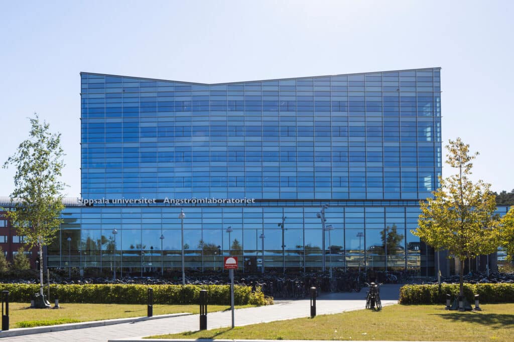
2026 05 01
Myfab Chalmers
,
Myfab
,
Myfab KTH
,
Myfab Lund
,
Myfab Uppsala
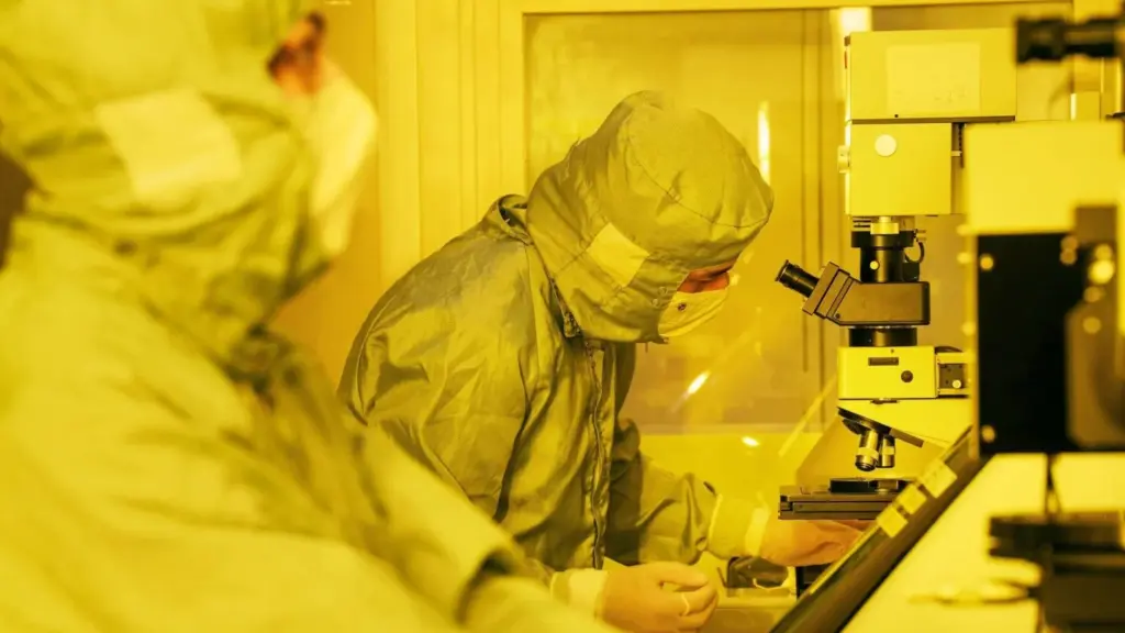
June 1-3: Nordic user meeting in Uppsala
Read more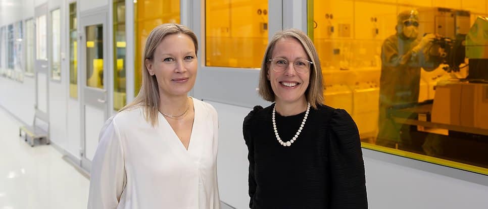
2026 04 27
Myfab Uppsala