Skip to content

Future engineers visit Myfab Uppsala

bachelor students from the Introduction to Engineering Physics course offered by the Faculty of Science and Technology at Uppsala University. Pictured here is just part of a larger group of around 60 curious and motivated future engineers.
Örjan Wallin

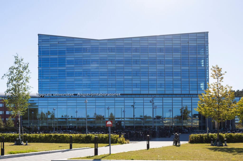
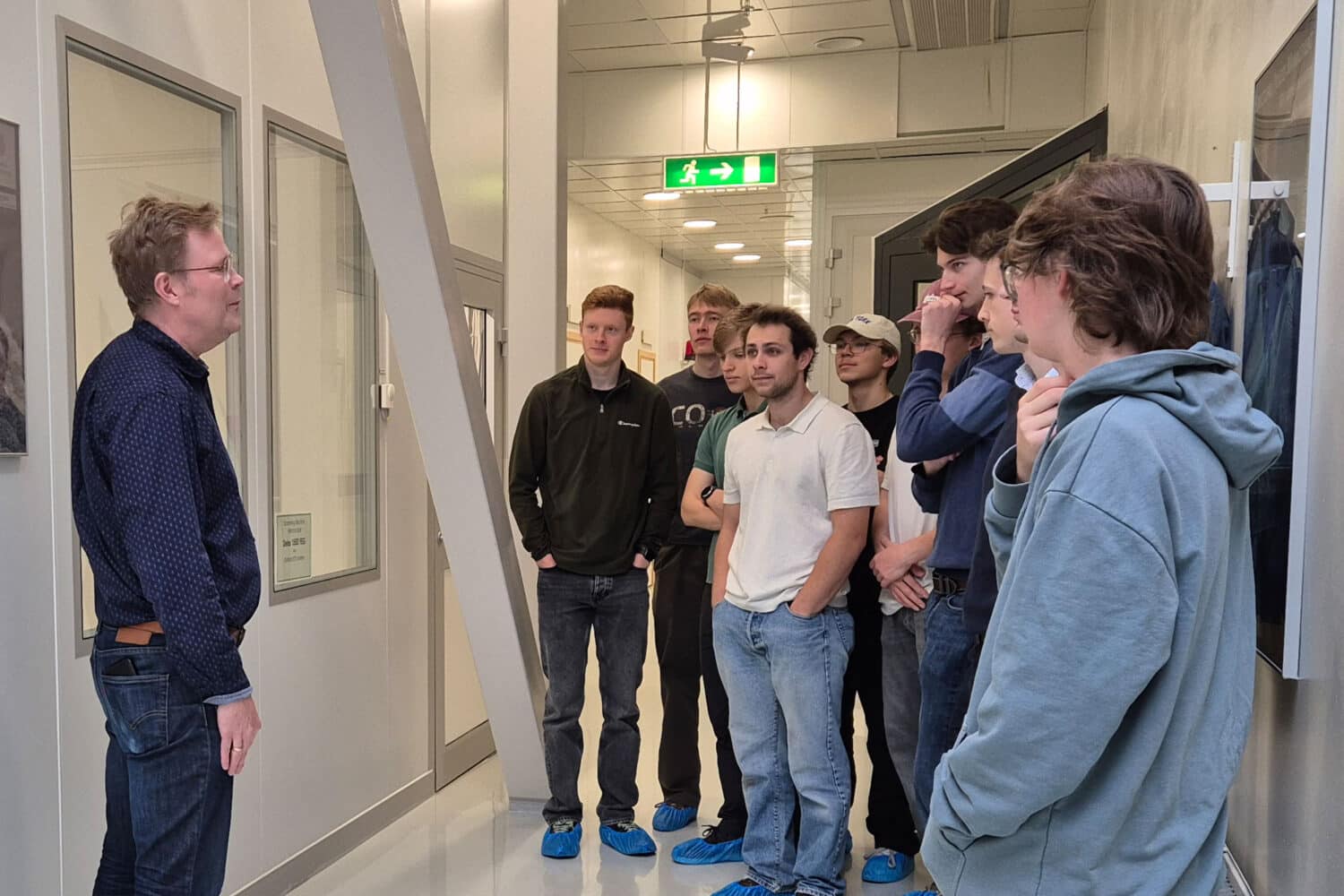
Today, Myfab Uppsala had the pleasure of hosting a group of enthusiastic bachelor students. Around 60 curious and motivated students visited our facilities to learn more about advanced research infrastructure and the practical applications of micro- and nanotechnology.

“It’s always a joy to meet young people with a genuine interest in science and technology. We hope today’s visit sparked curiosity,” said Stefan Nygren, Lab Manager at Myfab Uppsala.

The students are enrolled in the Introduction to Engineering Physics course, part of the Bachelor’s programme at Uppsala University’s Faculty of Science and Technology. The course introduces key concepts in physics, mathematics, and technology, and is coordinated by the Department of Electrical Engineering.
During the visit, students toured the cleanroom environment, attended presentations on ongoing research projects, and engaged in discussions with our experts.
Supporting education is part of our long-term vision. Inspiring the next generation of innovators starts here!

Highlights and events

The world’s first Arctic weather satellite was launched into orbit in 2024. Now, the Chalmers-based technology used in the satellite’s microwave radiometers will be deployed in Europe’s new weather satellite programme, EPS-Sterna. Image: European Space Agency
2026 03 27
Myfab Chalmers

Chalmers research at the heart of record order for Europe’s new weather satellites

Read more
Event
2026 03 23
Myfab Chalmers , Myfab , Myfab KTH , Myfab Lund , Myfab Uppsala

April 15: Myfab joins SEMICON 2026

Read more
The conceptual image shows how the researchers’ sculpted pattern of tiny hills and valleys – smaller than one millionth of a hair’s thickness – on the substrate (MgO, at the bottom) guides how the atoms in the superconducting material (YBCO, on top) settle. At the interface between the two layers, an electronic landscape allows superconductivity to occur at higher temperatures than previously possible – even when high magnetic fields were are applied. Credit: Chalmers University of Technology / Riccardo Arpaia
2026 03 18
Myfab Chalmers

Superconductor advance could unlock ultra-energy-efficient electronics

Read more
Event a university house - Ångström Laboratory - Myfab Uppsala
2026 03 12
Myfab Chalmers , Myfab , Myfab KTH , Myfab Lund , Myfab Uppsala

June 1-3: Nordic user meeting in Uppsala

Read more
See all highlights