Sweden’s news editorial SVT visited Myfab Chalmers, highlighting the high demand for Chalmers University’s dust-free lab in Gothenburg, which plays a crucial role in semiconductor research. Semiconductors are essential for modern technology, and Europe aims to reduce its dependence on Taiwan, China, and the USA.
As Europe aims to become more self-sufficient in semiconductor production, a special lab at Chalmers plays a key role. In a completely dust-free environment, researchers and companies develop semiconductor components that are fundamental to all modern technology. Interest in the lab is growing larger and larger.
In the summer of 2023, the EU adopted the Semiconductor Regulation – the so-called European Chips Act. The new rules aim to double the EU’s global market share for semiconductors from 10 percent to at least 20 percent by 2030.
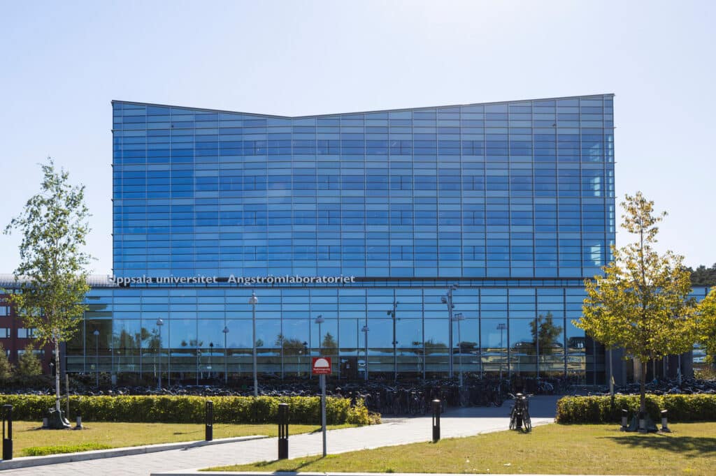
The cleanroom, which is likely to be Gothenburg’s and Western Sweden’s cleanest place, is part of Myfab. It is a national research resource that also includes three similar laboratories. These are located at the universities in Lund and Uppsala, as well as at KTH in Stockholm.
In the clip, you can follow along inside Chalmers’ cleanroom.
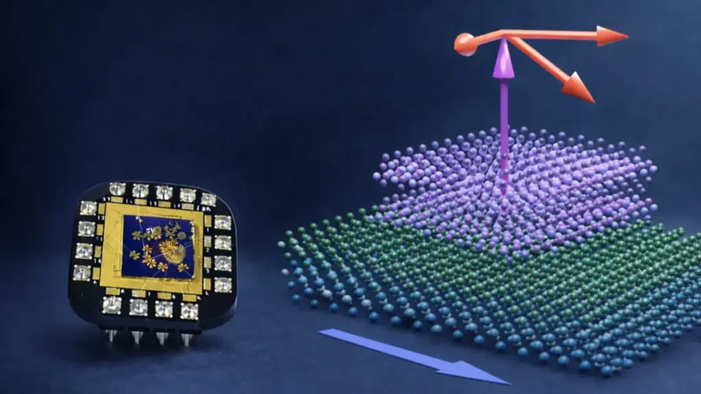
The chip often contains silicon, a so-called semiconductor material, which does not conduct electricity as well as conductors but does not completely exclude electrical conduction like an insulator.Common to many semiconductors is that part of the material is doped to create so-called pn-junctions.
There are many types of semiconductor components, the most common being diodes, transistors, and thyristors. The areas of application have increased as technology has developed.


