Skip to content

Innovative fabrication method for flat magnetic nanostructures

Four step process: 1. Sputtering, 2. Patterned mask, 3. Implantation, 4. Removal of mask

“These flat magnetic nanostructures present promising potential for advanced applications, including in-material computation, that is that the material itself can function as a computer, processing and calculating solutions internally, making certain types of problem-solving faster and more efficient”, says Christina Vantaraki, PhD student at the Department of Physics and Astronomy and the developer of the method.

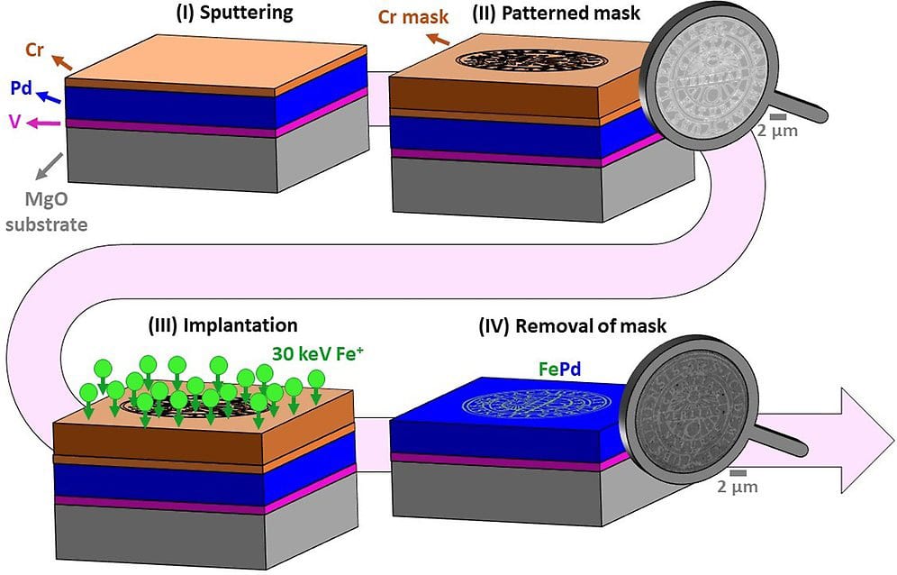
This new way of designing nano magnets was supported through resources at the Materials Physics Division of the Department of Physics and Astronomy, MyFab Uppsala, and the Tandem Laboratory and was achieved in four steps.

Highlights and events

bachelor students from the Introduction to Engineering Physics course offered by the Faculty of Science and Technology at Uppsala University. Pictured here is just part of a larger group of around 60 curious and motivated future engineers.
2025 10 01
Myfab Uppsala

Future engineers visit Myfab Uppsala

Read more
The material features a magnetic alloy made from both magnetic and non-magnetic elements (cobalt, iron, germanium and tellurium), allowing ferromagnetism and antiferromagnetism to coexist within a sin
2025 09 26
Myfab Chalmers

Material breakthrough paves way for major energy savings in memory chips

Read more
At the event: Peter Modh, Chalmers - Vanya Darakchieva, Lund University - Mikael Östling, KTH
2025 09 24
Myfab , Myfab Chalmers , Myfab KTH , Myfab Lund

Inauguration – WBG Pilot Line

Read more
The second gear from the right has an optical metamaterial that react to laserlight and makes the gear move. All gears are made in silica directly on a chip. Each gear is about 0.016 mm in diameter.
2025 09 22
Myfab Chalmers

Light-powered motor fits inside a strand of hair

Read more
See all highlights