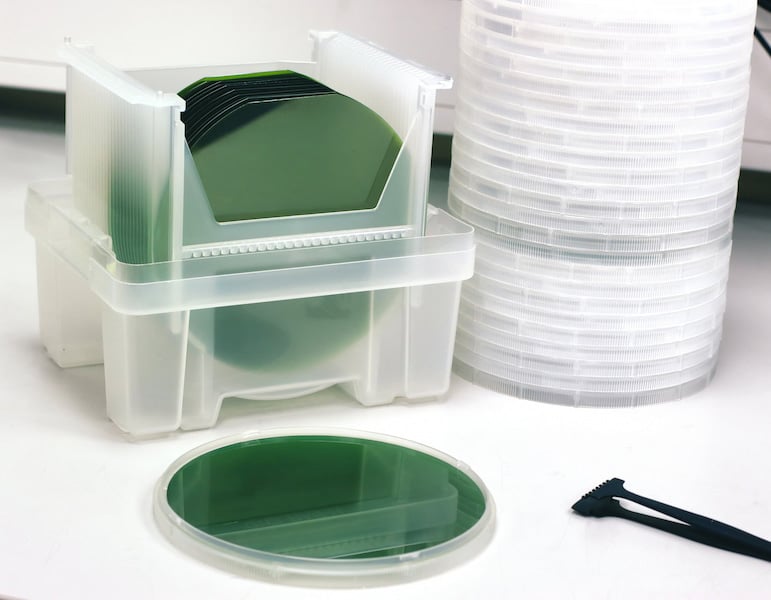
Kiselkarbid i Stockholm AB (KISAB), a materials company based in Kista, is working to develop next‑generation 8‑inch silicon carbide substrates – a material increasingly in demand as industries shift toward electrification. Larger substrates with lower defect densities are considered essential for improving the performance and lowering the cost of technologies such as electric vehicles, charging infrastructure and renewable‑energy systems.
A growing company addressing a global need
Founded in 2017, KISAB was created by a team of materials specialists who identified a clear gap in the semiconductor market: very few companies worldwide have the capability to produce large, high‑quality silicon carbide wafers. From its facility in Kista, the company has grown steadily and today employs 16 people. With its focus on scaling production volume, KISAB aims to support the rapid expansion of energy‑efficient electronics.
Myfab KTH /Electrum Laboratory plays a key role
For a young company working with advanced materials, access to the right infrastructure is crucial. According to KISAB, the greatest benefit of using the Electrum Laboratory cleanroom – part of the Myfab national research network – is gaining access to sophisticated, high‑cost tools that would be impossible for a start‑up to purchase on its own.
Beyond equipment, cleanroom access supports KISAB’s development work in three critical ways. First, the lab provides the specialized tools required to process and evaluate silicon carbide materials with precision. Second, the environment brings KISAB into close contact with skilled researchers whose expertise contributes directly to faster problem‑solving and improved development outcomes. Finally, when technical issues arise, Electrum’s staff offer hands‑on support, helping to troubleshoot tool failures and keep experiments on track.
Accelerating progress toward energy‑efficient technology
Together, these resources allow KISAB to shorten development cycles and reduce risk. As global demand for efficient power electronics continues to grow, the company expects its 8‑inch silicon carbide substrates to play an important role in enabling the next wave of clean‑energy technology.