Skip to content

Myfab Labs

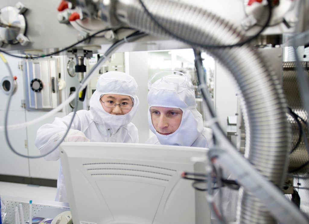
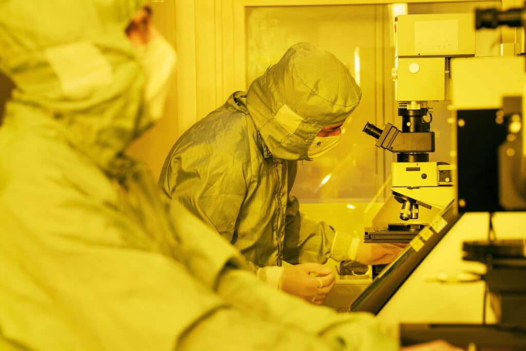
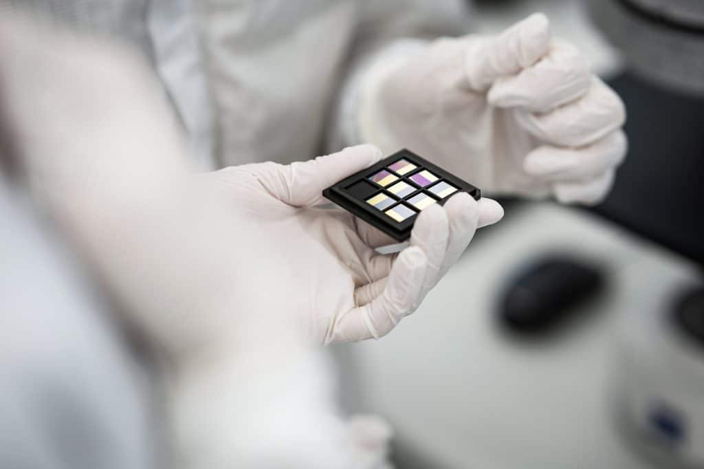
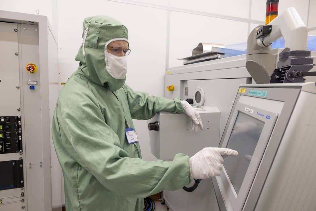
Myfab’s various laboratories are partly specialised in different application areas and their related processes and material systems. This diversity of expertise creates a synergistic environment where the unique strengths of each lab complement one another, driving innovation and advancing research.

As a Myfab user, you gain access to a comprehensive suite of resources and expertise across all these labs, facilitating cutting-edge research and development in various scientific domains.

Our labs

Chalmers logotyp
Cleanroom MC2, two people wearing protective gear and looking at a screen

Myfab Chalmers

Specializes in advanced semiconductor processing, focusing on deep silicon etching, high-aspect ratio geometries, 3D MEMS devices, and high-power electronics.

Go to Myfab Chalmers
KTH logotype
Person working while wearing protective gear, their silhouette reflected in glass

Myfab KTH

Specializes in nano and micro-scale fabrication, featuring silicon FDSOI and SiC device lines, and supports research in MEMS, photonics, 2D materials, and nano-scale research. It also hosts several semiconductor tech companies.

Go to Myfab KTH
Lunds university logotype
Closeup of object helt with protective gloves

Myfab Lund

Specializes in epitaxial growth and synthesis of compound semiconductor materials, enabling advanced research in quantum technology, novel materials, sustainable energy, semiconductor technology (vertical nanowire transistors and PV), wide band gap materials, and precision medicine.

Go to Myfab Lund
Uppsala university logotype
Person wearing protective gear interacting with a screen of a big machine

Myfab Uppsala

Supports interdisciplinary research in materials science, nanoscience, ICT, bionanotechnology, life sciences, energy research, and micronanosystems.

Go to Myfab Uppsala