Skip to content

Launch of WiTECH – A milestone for wireless and semiconductor innovation

Group mingling at the Launch of WiTech event

WiTECH, Wireless Infrastructure Technology at Chalmers, organises a full day for its partners to present research projects and discuss long-term strategy for the centre. The newly established WiTECH competence centre, hosted by the Department of Electrical Engineering (E2) in close collaboration with the Department of Microtechnology and Nanoscience (MC2), intends to be a key player in creating a sustainable future by:

  • Developing next generation of robust and trustworthy wireless communication and sensor systems (e.g., the sixth-generation wireless telecommunication 6G); and
  • Sustainable, energy-efficient semi-conductor components and processes.

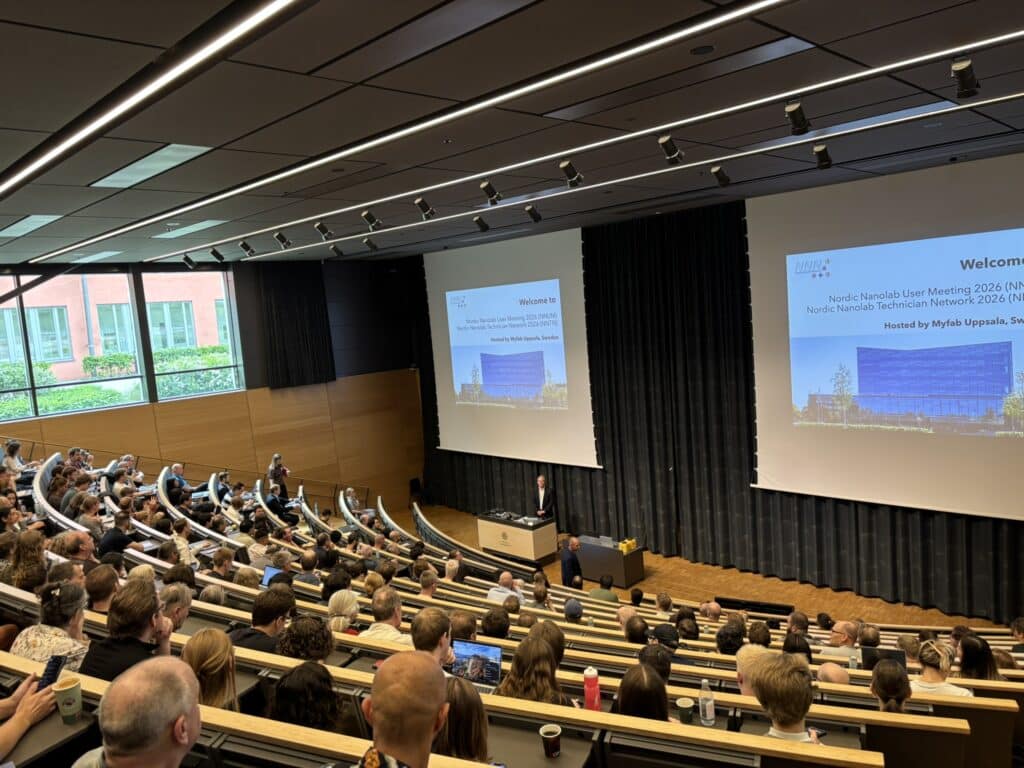
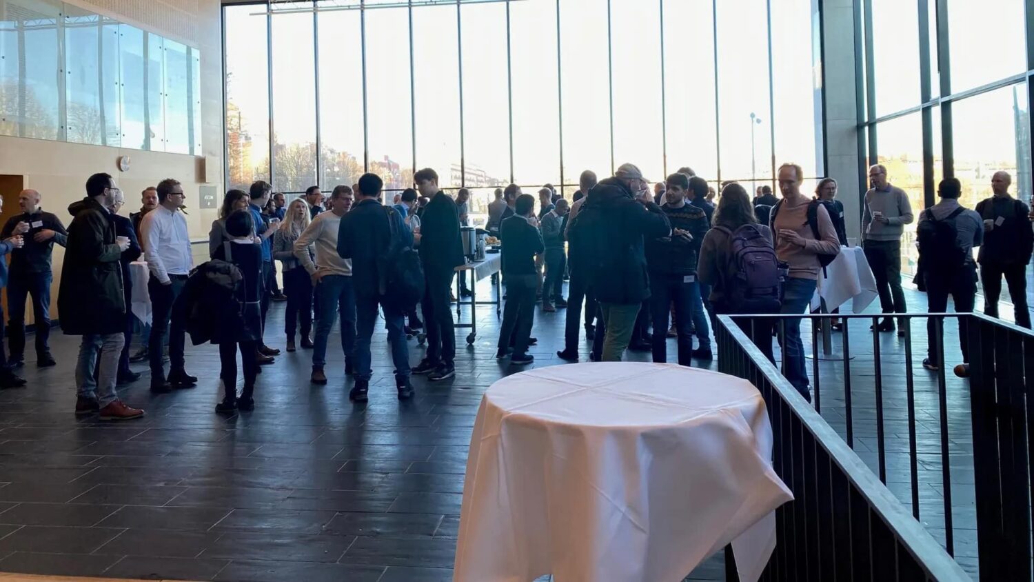
The first physical event brough together the entire WiTECH centre consortium with nearly 100 participants from 17 partners, including Ericsson, SAAB, Volvo Cars, Gapwaves, Gotmic, Icomera, Mitsubishi Electric Corporation, Kongsberg, Low Noise Factory, AAC Clyde Space Omnisys, Qamcom, RISE, Satcube, UMS, UniqueSec, Virginia Diodes, and Chalmers. Students at Chalmers and Vinnova representative also attended this event.

At the event multiple operational and research activities were finalized that are necessary to set the course for a successful collaboration. The leading representatives of all 17 partners gathered to start the collaboration.

Highlights and events

The world’s first Arctic weather satellite was launched into orbit in 2024. Now, the Chalmers-based technology used in the satellite’s microwave radiometers will be deployed in Europe’s new weather satellite programme, EPS-Sterna. Image: European Space Agency
2026 03 27
Myfab Chalmers

Chalmers research at the heart of record order for Europe’s new weather satellites

Read more
Event
2026 03 23
Myfab Chalmers , Myfab , Myfab KTH , Myfab Lund , Myfab Uppsala

April 15: Myfab joins SEMICON 2026

Read more
The conceptual image shows how the researchers’ sculpted pattern of tiny hills and valleys – smaller than one millionth of a hair’s thickness – on the substrate (MgO, at the bottom) guides how the atoms in the superconducting material (YBCO, on top) settle. At the interface between the two layers, an electronic landscape allows superconductivity to occur at higher temperatures than previously possible – even when high magnetic fields were are applied. Credit: Chalmers University of Technology / Riccardo Arpaia
2026 03 18
Myfab Chalmers

Superconductor advance could unlock ultra-energy-efficient electronics

Read more
Event a university house - Ångström Laboratory - Myfab Uppsala
2026 03 12
Myfab Chalmers , Myfab , Myfab KTH , Myfab Lund , Myfab Uppsala

June 1-3: Nordic user meeting in Uppsala

Read more
See all highlights