Skip to content

Miniature laser technology could bring lab testing into your home

A research team at Chalmers University of Technology has developed a new diminutive laser technology that makes it possible to create a miniature biosensor with the laser source and optics integrated onto a one-centimetre semiconductor chip. This enables significantly smaller sensors, paving the way for portable optical technology and for moving certain types of medical sampling from hospitals to the patients’ homes. Illustration: Chalmers/Erik Strandberg

A research team at Chalmers University of Technology, Sweden, has developed new laser technology that could lead to tiny, cost-effective biosensors. The sensors integrate lasers and optics together on a centimeter-sized chip, which could move testing from hospitals to patients’ homes. This, in turn, would free up hospital beds and reduce visits to clinics.

By studying how various biomolecules interact with each other – for example antibodies in the immune system and xenobiotic antigens – researchers can gain valuable insights leading to new medicines and vaccines or assess whether a sample contains signs of infection.

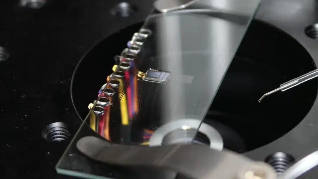
Optical biosensors based on a technique called surface-plasmon resonance are an important tool used for studying these types of interactions. The sensors direct light onto a gold surface and measure minuscule changes in the light’s reflection when biomolecules are placed on the surface.

Now, a research team at Chalmers is announcing a new laser technology that makes it possible to create such biosensors in a miniature format. The laser source and the necessary optics are directly integrated onto a semiconductor chip, allowing for significantly more compact sensors. This opens the door to making optical sensing technology portable and applicable outside the laboratory environment.

Highlights and events

2026 06 03
Myfab , Myfab Chalmers , Myfab KTH , Myfab Lund , Myfab Uppsala

Nordic Nanolab meeting reaches record-high attendance

Read more
2026 05 27
Myfab , Myfab Chalmers , Myfab KTH , Myfab Lund , Myfab Uppsala

New report highlights the need to strengthen Sweden’s semiconductor ecosystem

Read more
2026 05 12
Myfab , Myfab Chalmers , Myfab KTH , Myfab Lund , Myfab Uppsala

Excellence cluster applications – Myfab plays a key role

Read more
2026 05 07
Myfab

Europe’s nanofabrication network, EuroNanoLab, meets in Leuven

Read more
See all highlights