Skip to content

Nanoscale movies show how to build new materials

The studies of existing materials are the first step on the way to designing completely new structures with new properties. Photo: KAW / Kennet Ruona

By studying how materials build themselves and by mimicking those processes, it is possible to create materials with new structures and properties. This is what Wallenberg Scholar Kimberly Dick Thelander, professor of materials science at Lund University, is doing.

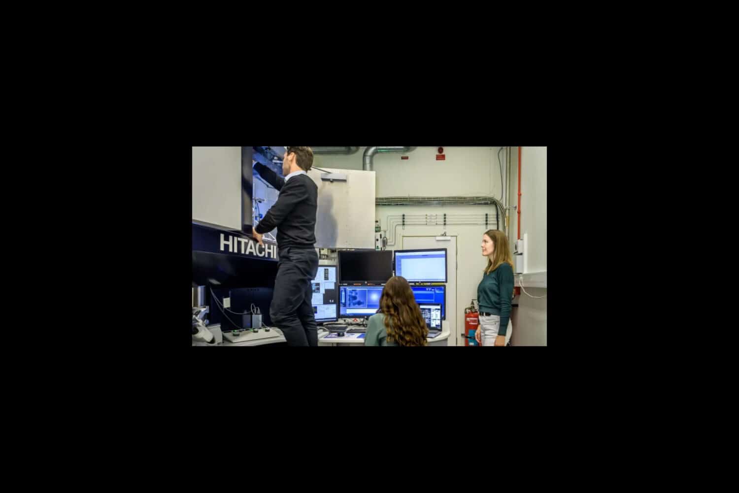
At the nano scale, which is measured in billionths of a meter, phenomena occur that do not otherwise exist. Thelander and her colleagues are studying this process while it actually takes place. This is possible thanks to an electron microscope she has been using and developing since 2016.

“Everything we wanted to do when it was new is now possible. We use the microscope every day, and it is involved in about 70 percent of our research,” she says.

The studies of existing materials are the first step on the way to designing completely new structures with new properties.

The basic material is usually a gas that spontaneously forms crystals inside a large machine. The machine contains the electron microscope, enabling the researchers to record images and film at atomic scale.

“We’re trying to understand the materials and their crystalline structures at atomic level. When we identify the processes that determine the structures and control those processes, we will also be able to control the properties.”

Highlights and events

The world’s first Arctic weather satellite was launched into orbit in 2024. Now, the Chalmers-based technology used in the satellite’s microwave radiometers will be deployed in Europe’s new weather satellite programme, EPS-Sterna. Image: European Space Agency
2026 03 27
Myfab Chalmers

Chalmers research at the heart of record order for Europe’s new weather satellites

Read more
Event
2026 03 23
Myfab Chalmers , Myfab , Myfab KTH , Myfab Lund , Myfab Uppsala

April 15: Myfab joins SEMICON 2026

Read more
The conceptual image shows how the researchers’ sculpted pattern of tiny hills and valleys – smaller than one millionth of a hair’s thickness – on the substrate (MgO, at the bottom) guides how the atoms in the superconducting material (YBCO, on top) settle. At the interface between the two layers, an electronic landscape allows superconductivity to occur at higher temperatures than previously possible – even when high magnetic fields were are applied. Credit: Chalmers University of Technology / Riccardo Arpaia
2026 03 18
Myfab Chalmers

Superconductor advance could unlock ultra-energy-efficient electronics

Read more
Event a university house - Ångström Laboratory - Myfab Uppsala
2026 03 12
Myfab Chalmers , Myfab , Myfab KTH , Myfab Lund , Myfab Uppsala

June 1-3: Nordic user meeting in Uppsala

Read more
See all highlights