In a significant move to bolster the nation’s semiconductor industry, the Myfab laboratories have been awarded substantial funding through a new initiative by the Swedish Agency for Economic and Regional Growth. This initiative aims to enhance the semiconductor ecosystem across Sweden and further strengthen the Swedish participation in the Chips Joint Undertaking.
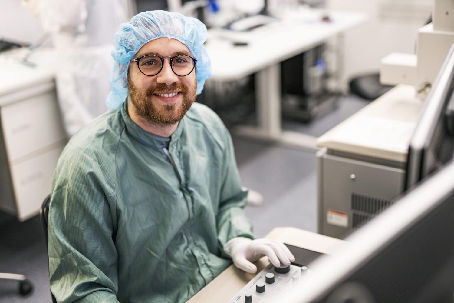
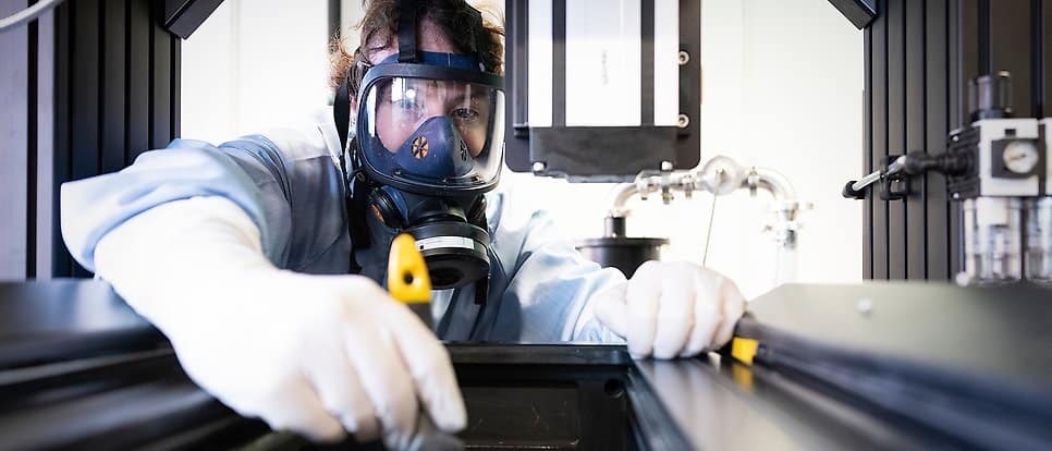
The Myfab laboratories receive funding to develop processes, methods, and services, specifically targeting Small and Medium Enterprises (SMEs). This includes enhancing SME onboarding and investing in advanced equipment. These measures will support innovation and development in the semiconductor sector, improve sustainability, and make the laboratories’ resources more accessible and reliable for users.
Myfab’s lab receives four out of six approved projects. In addition to the funding from the Swedish Agency for Economic and Regional Growth, each project has co-financing from regional and national actors.
Funding to each node 2025-2028:
- Myfab Chalmers: 4,2 MSEK, Myfab Chalmers för svensk halvledarinnovation
- Myfab KTH: 4,9 MSEK, Semiconductor Arena (Kista Science City)
- Myfab Lund: 12 MSEK, Myfab Lund för svensk halvledarinnovation
- Myfab Uppsala: 14,9 MSEK, Myfab Uppsala för svensk halvledarinnovation
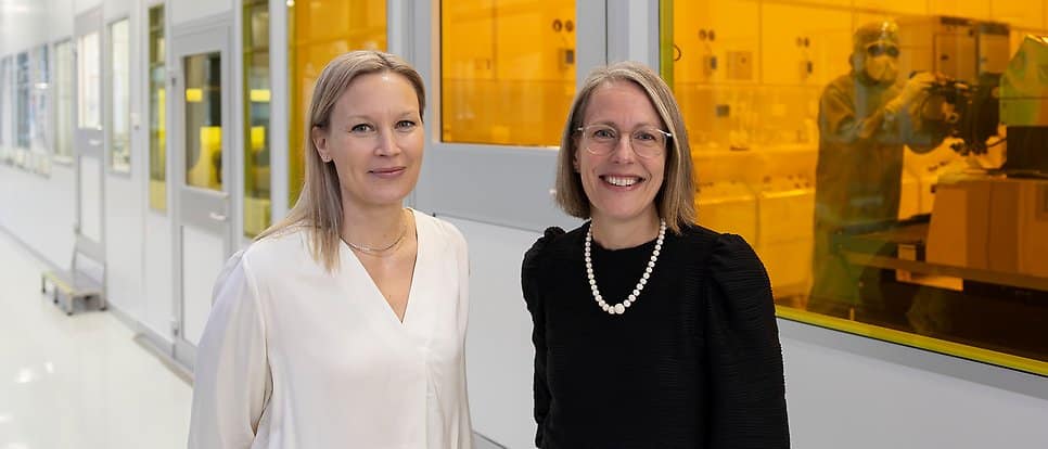
Semiconductors are vital for digitalization, electrification, and climate transition. The semiconductor sector is rapidly evolving and crucial globally. Sweden’s expertise in this knowledge-intensive field fosters innovation and drives economic growth. Myfab plays a central role in this context by offering advanced laboratory resources and support to research and development.
Contacts:
Myfab Chalmers: Peter Modh, +46 31 772 1605, peter.modh@chalmers.se
Myfab KTH: Carina Zaring, +46 8 790 4388, caza@kth.se
Myfab Lund: Luke Hankin, +46 222 3647, luke.hankin@ftf.lth.se
Myfab Uppsala: Stefan Nygren, +46 18 471 3100, stefan.nygren@Angstrom.uu.se
Press release: Stora satsningar på halvledare – Sverige stärker sitt ekosystem för framtidens industri – Tillväxtverket


