Skip to content

Semi-conductor technology from Chalmers on board first Arctic weather satellite

Arctic satellite in space above earth

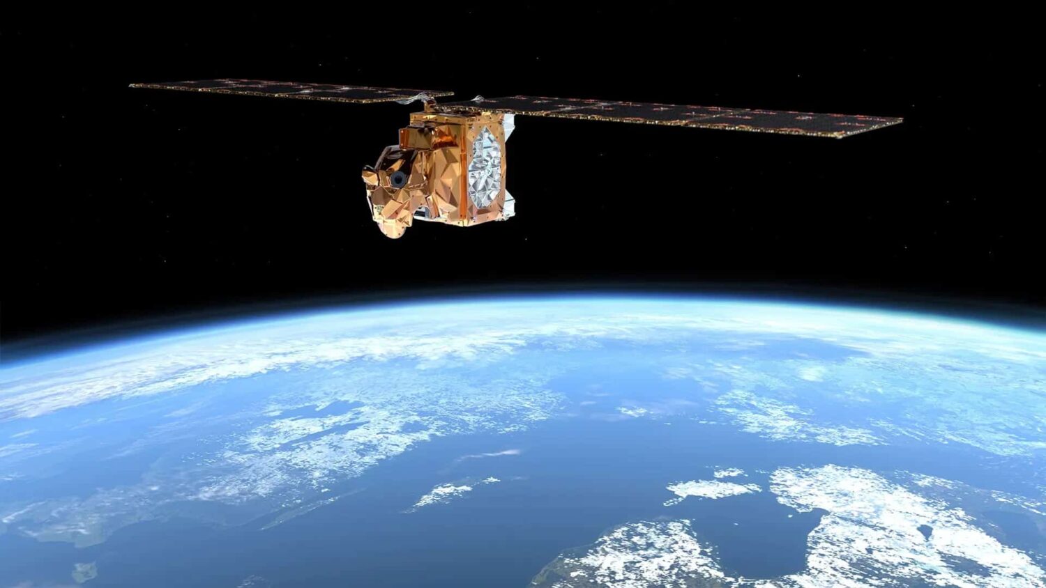
With only 125 kilos in weight – and as small as the size of a dishwasher – the first Arctic Weather Satellite, AWS, has successfully been launched with the mission to provide better weather forecasts for the Arctics, a region severely affected by climate change. The small satellite is equipped with a 19-channel cross-track microwave radiometer using semi-conductor technology fabricated at Chalmers University of Technology.

The new Arctic weather satellite, AWS, was lofted into orbit on 16 August at 20:56 CEST aboard a SpaceX Falcon 9 rocket from the Vandenberg Space Force Base in California, just north of Los Angeles. About six hours later, the KSAT ground station in Svalbard, Norway, received the all-important signal indicating the satellite’s safe arrival in orbit.

With a mission to collect important data on moisture and temperature levels in the Earth’s atmosphere, and measure the amount of ice in clouds, the satellite is sent off to enhance our understanding of the weather conditions at the poles. The clouds, and what happens inside them, are important parameters when trying to predict climate change.

Highlights and events

The conceptual image shows how the researchers’ sculpted pattern of tiny hills and valleys – smaller than one millionth of a hair’s thickness – on the substrate (MgO, at the bottom) guides how the atoms in the superconducting material (YBCO, on top) settle. At the interface between the two layers, an electronic landscape allows superconductivity to occur at higher temperatures than previously possible – even when high magnetic fields were are applied. Credit: Chalmers University of Technology / Riccardo Arpaia
2026 03 18
Myfab Chalmers

Superconductor advance could unlock ultra-energy-efficient electronics

Read more
Event a university house - Ångström Laboratory - Myfab Uppsala
2026 03 12
Myfab Chalmers , Myfab , Myfab KTH , Myfab Lund , Myfab Uppsala

Nordic user meeting: NNTN & NNUM in Uppsala

Read more
Illustration of the device concept. A memory chip based on stacked quantum materials. By placing a magnetic layer on top of a topological material, the researchers were able to switch magnetization using very small electrical currents and without applying an external magnetic field. Illustration: Lalit Pandey
2026 03 11
Myfab Chalmers

Quantum materials breakthrough for energy-efficient data processing

Read more
Ove Öhman has been a bridge-builder between academia and the business sector for several decades and has helped strengthen Uppsala’s innovation environment. Photo: Mikael Wallerstedt, Uppsala University
2026 03 10
Myfab Uppsala

Ove Öhman receives prize as a bridge-builder between research and innovation

Read more
See all highlights