Skip to content

Innovative fabrication method for flat magnetic nanostructures

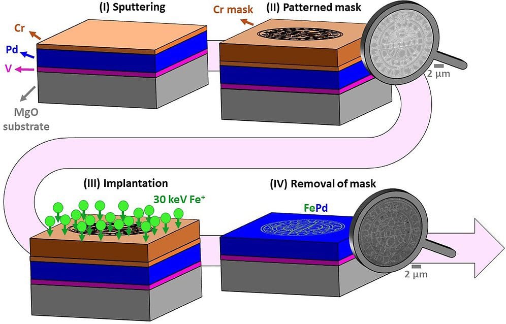
Four step process: 1. Sputtering, 2. Patterned mask, 3. Implantation, 4. Removal of mask

“These flat magnetic nanostructures present promising potential for advanced applications, including in-material computation, that is that the material itself can function as a computer, processing and calculating solutions internally, making certain types of problem-solving faster and more efficient”, says Christina Vantaraki, PhD student at the Department of Physics and Astronomy and the developer of the method.

This new way of designing nano magnets was supported through resources at the Materials Physics Division of the Department of Physics and Astronomy, MyFab Uppsala, and the Tandem Laboratory and was achieved in four steps.

Highlights and events

Meeting Closeup image with sharp green light
2025 03 25
Myfab

April 8-9: Nordic Nanolab Network (NNN)

Read more
Person in protective gear smiling while sitting down in front of a machine control panel
2025 03 06
Myfab Chalmers , Myfab KTH , Myfab Lund , Myfab Uppsala

Myfab labs receive funding to strengthen the semiconductor ecosystem

Read more
Vanya Darakchieva and Andri Dhora work on the PLD apparatus. Photo: Jenny Leyman
2025 03 06
Myfab , Myfab Lund

“Research chef” refines the recipe for semiconductors

Read more
Electron microscopy image of algae sitting on the nanowires. Picture: Martin Hjort
2025 03 05
Myfab , Myfab Lund

Making conductive polymer nanowires to probe cells

Read more
See all highlights