Skip to content

April 15: Myfab joins SEMICON 2026

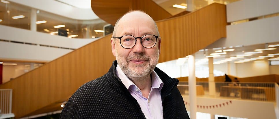
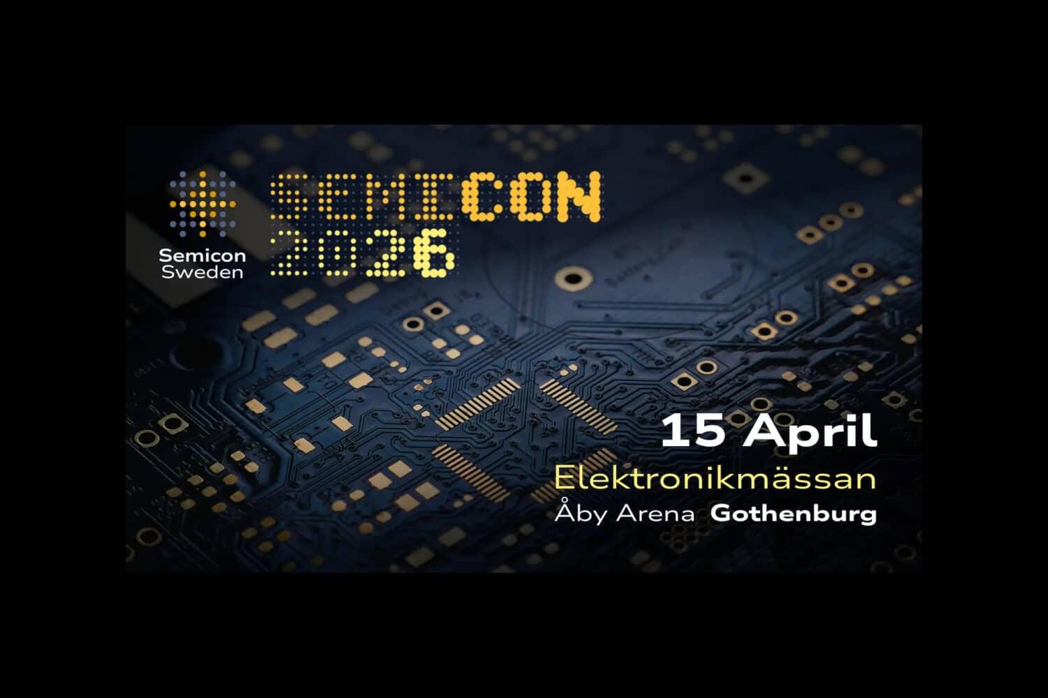
Myfab Director Thomas Swahn will speak at SEMICON 2026, taking place on 15 April at Åby Arena in Gothenburg. The conference is co-located with Elektronikmässan, Sweden’s leading electronics trade fair, which offers free visitor admission. This gives SEMICON participants expanded access to exhibitors, technologies, and networking opportunities across the broader electronics value chain.

Thomas will present during the Enabling capabilities session, where he will introduce Myfab – Sweden’s national research infrastructure for micro- and nano fabrication. His talk is scheduled for 14:10–14:30 and will highlight Myfab’s role in strengthening Sweden’s position in advanced semiconductor research and fabrication, as well as its contribution to Europe’s broader microelectronics ambitions.

SEMICON 2026 brings together leaders from industry, academia, government, and research institutes to discuss Sweden’s strategic role in the European semiconductor landscape. This year’s programme includes topics such as Sweden’s national semiconductor strategy, the EU Chips Act, and emerging opportunities for cooperation across the value chain.

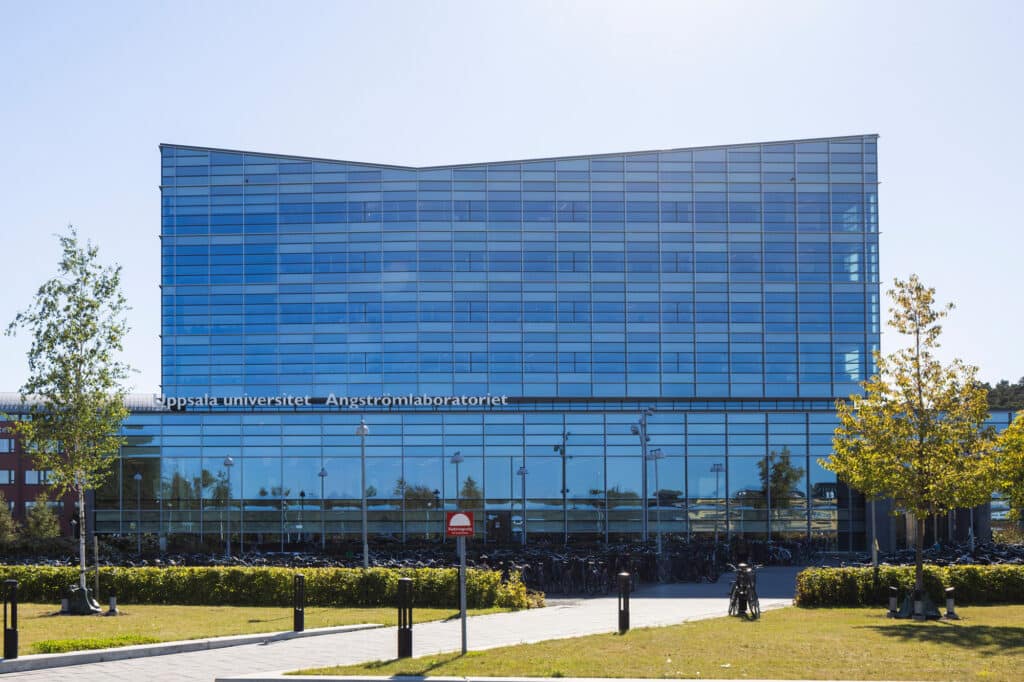
With Myfab representing a cornerstone of Sweden’s research capabilities, Thomas Swahn’s participation underscores the infrastructure’s importance in enabling innovation, supporting talent development, and accelerating technological progress within the semiconductor field.

Highlights and events

The conceptual image shows how the researchers’ sculpted pattern of tiny hills and valleys – smaller than one millionth of a hair’s thickness – on the substrate (MgO, at the bottom) guides how the atoms in the superconducting material (YBCO, on top) settle. At the interface between the two layers, an electronic landscape allows superconductivity to occur at higher temperatures than previously possible – even when high magnetic fields were are applied. Credit: Chalmers University of Technology / Riccardo Arpaia
2026 03 18
Myfab Chalmers

Superconductor advance could unlock ultra-energy-efficient electronics

Read more
Event a university house - Ångström Laboratory - Myfab Uppsala
2026 03 12
Myfab Chalmers , Myfab , Myfab KTH , Myfab Lund , Myfab Uppsala

June 1-3: Nordic user meeting in Uppsala

Read more
Illustration of the device concept. A memory chip based on stacked quantum materials. By placing a magnetic layer on top of a topological material, the researchers were able to switch magnetization using very small electrical currents and without applying an external magnetic field. Illustration: Lalit Pandey
2026 03 11
Myfab Chalmers

Quantum materials breakthrough for energy-efficient data processing

Read more
Ove Öhman has been a bridge-builder between academia and the business sector for several decades and has helped strengthen Uppsala’s innovation environment. Photo: Mikael Wallerstedt, Uppsala University
2026 03 10
Myfab Uppsala

Ove Öhman receives prize as a bridge-builder between research and innovation

Read more
See all highlights