Microscopic labs that deliver test results cheaply, quickly and efficiently – in research, business contexts or health services. This is the theme running through Ove Öhman’s entrepreneurship. In April 2026 he will receive Uppsala University’s Innovation and Entrepreneurship Award.
The citation states that Ove Öhman “has been a bridge-builder between academia and the business sector for several decades and has helped strengthen Uppsala’s innovation environment.”
In collaboration with companies and researchers in Uppsala, he has built up a technology that has been successfully used for purposes such as protein analysis and for rapidly determining which type of antibiotic should be used for different bacteria.
“The common theme is microfluidics and doing really tiny things – a kind of plumbing on a small scale,” Öhman explains.
From silicon to plastic
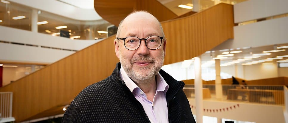
Ove Öhman came to Uppsala in the 1980s with a Master of Science Degree in Engineering from Linköping University. He obtained a job at Pharmacia’s spin-off company Biacore, which was developing new technology for protein analysis. Öhman’s mission was to see whether semiconductor technology could also be used to channel fluids, not just electrons.
He registered for a course in micromechanics at Uppsala University and began to etch patterns in silicon wafers for microscopic experiments, a technology known as microfluidics. Fairly soon, he and his colleagues realised that it would be better to use plastic materials, which are less fragile and cheaper. The inspiration came from an unexpected direction.
“I was reading an article in the magazine Ny Teknik about how a CD is manufactured and I saw that this plastic disc looked more or less like the silicon wafer I was etching. I thought, if I use the same process, perhaps I can produce the pattern in plastic instead,” Öhman recalls.