
In a significant move to bolster the nation’s semiconductor industry, the Myfab laboratories have been awarded substantial funding through a new initiative by the Swedish Agency for Economic and Regional Growth. This initiative aims to enhance the semiconductor ecosystem across Sweden and further strengthen the Swedish participation in the Chips Joint Undertaking.

It has been decided that Vectura Fastigheter will host Myfab Lund's Nanolab Science Village, a lab for manufacturing nanomaterials and semiconductor components. The lab will be a neighbour of the major research facilities ESS and MAX IV, and together they will form a hub of scientific facilities that will create a competitive research environment with great opportunities.

We are very happy to announce that Lund Nano Lab (LNL) has been selected as one of three new Lund University Core Facilities

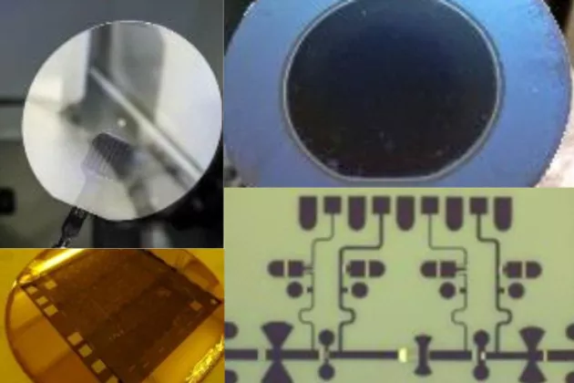
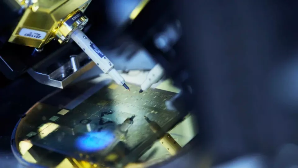
Myfab Lund is now the very proud owner of a brand new state-of-the-art Bruker D8 Discover X-ray Diffraction System (XRD).
Myfab Lund, Chalmers and KTH been invited to be part of a pilot line for Wide Bandgap materials, together with Linköping.
Welcome to an information meeting about Lund Nano Lab (LNL) – what is it, what does it offer and how can you access it? We will also tell you about the plans and process of building the new Nano Lab at Science Village, a cutting-edge semiconductor nanofabrication facility near MAX IV and ESS.
Sarah McKibbin gets funding for "Greening" Myfab Lund
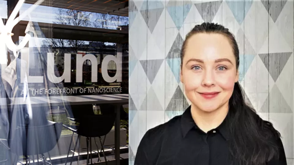
Optimise lab routines, minimise unnecessary consumption of lab consumables, recycle when possible, and improve user behaviour. That’s some of the improvements that can make the Lund Nano Lab greener, according to the project that Sarah McKibbin gets funding for, from the Lund University Sustainability Fund.
Compound Semiconductor Week (CSW) is the premier conference in the field of science, technology, and applications of compound semiconductors, and it will be arranged in Lund on 3–6 June 2024.

Prime Minister Ulf Kristersson visited NanoLund for a tour of the nano lab, discussions on how to make science, technology, engineering, and maths education more popular, to learn more about semiconductors and the technology behind them.
Vanya Darakchieva, Professor of Semiconductor Materials, and Heiner Linke, Professor of Nanophysics, have been named Wallenberg Scholars, a programme funded by the Knut and Alice Wallenberg Foundation that supports excellent basic research, primarily in medicine, technology, and natural sciences. In addition, three current Wallenberg Scholars in our research environment receive grants: Anne L’Huillier, Kimberly Dick Thelander, and Stephanie Reimann.
The five-year grant amounts to SEK 18 million each for researchers in theoretical subjects and up to SEK 20 million each for experimental subjects. As Nobel Prize laureate, Anne L’Huillier receives a grant of SEK 40 million.
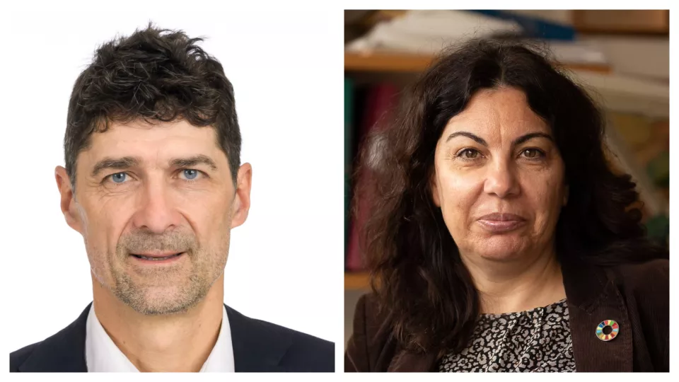
Semiconductors – the “brains” behind electronic products and systems. Whether mobile phones, automotive, energy, home appliances, or artificial intelligence, these components (“chips”) play a key role. At the same time, Asian countries account for more than half of the world’s semiconductor chip production. Swedish semiconductor capability is now to be strengthened by Lund University together with Chalmers and KTH
WISE, the Wallenberg Initiative Materials Science for Sustainability, is the largest-ever investment in materials science in Sweden and is financed by the Knut and Alice Wallenberg Foundation. WISE is now investing 500 million SEK (45 million Euros) for equipment and infrastructure at seven universities in Sweden to establish a national infrastructure for research into sustainable materials. 44 million SEK are dedicated to Myfab Lund and a further 21 MSEK to KTH.