Skip to content

Unique nanodisk pushing photonic research forward

Closeup of nanodisk

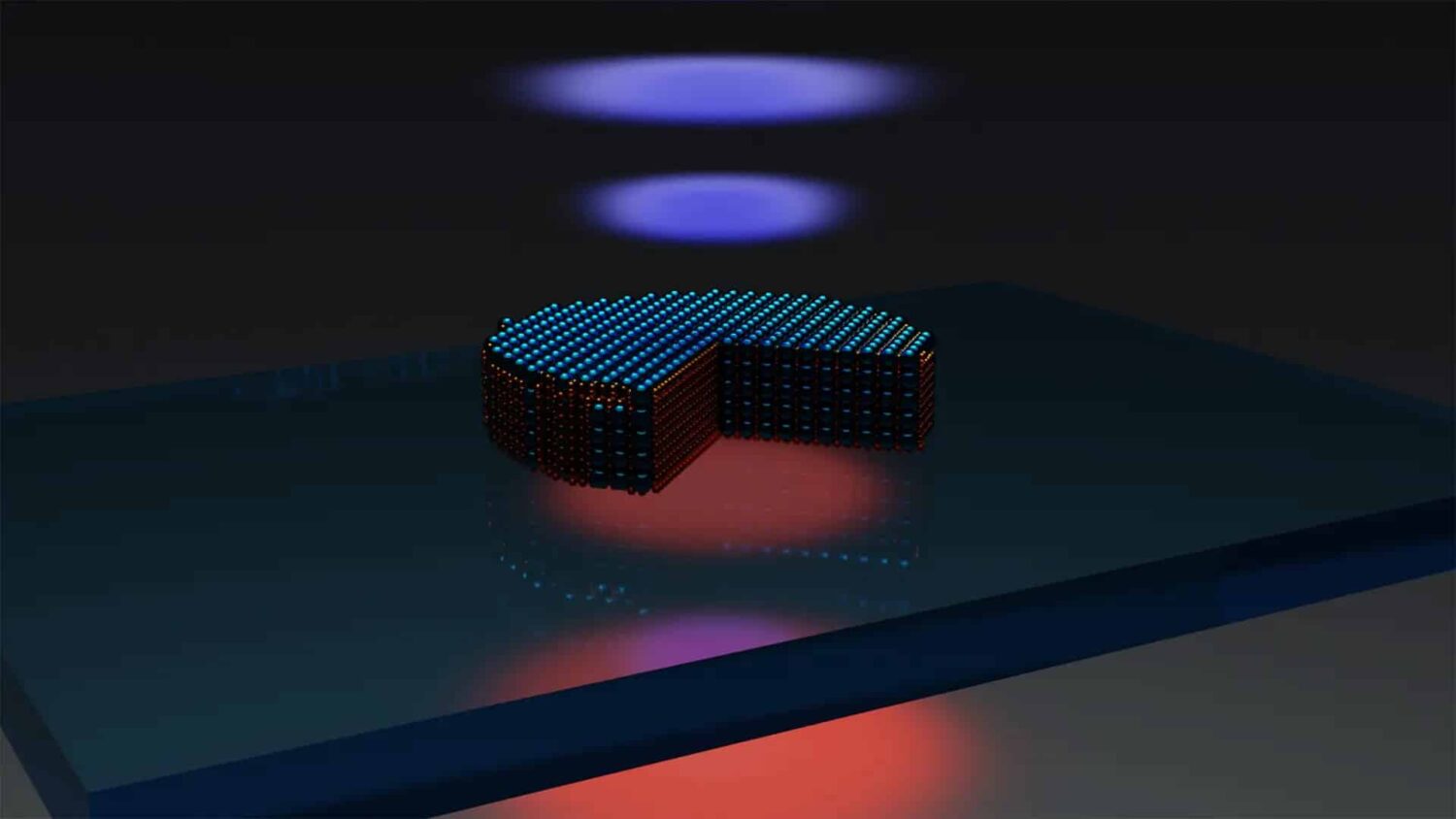
Researchers at Chalmers University of Technology have for the first time succeeded in combining two major research fields in photonics by creating a nanoobject with unique optical qualities. Since the object is a thousand times thinner than the human hair, yet very powerful, the breakthrough has great potential in the development of efficient and compact nonlinear optical devices.
“My feeling is that this discovery has a great potential,” says Professor Timur Shegai, who led the study at Chalmers.

Photonic applications harness the power of light-matter interactions to generate various intriguing phenomena. This has enabled major advances in communications, medicine, and spectroscopy, among others, and is also used in laser and quantum technologies. Now, researchers at the Department of Physics at Chalmers University of Technology have succeeded in combining two major research fields – nonlinear and high-index nanophotonics – in a single disk-like nanoobject.

“We were amazed and happy by what we managed to achieve. The disk looking structure is much smaller than the wavelength of light, yet it’s a very efficient light frequency converter. It is also 10,000 times, or maybe even higher, more efficient than the unstructured material of the same kind, proving that nano structuring is the way to boost efficiency,” says doctor Georgii Zograf, lead author of the article in Nature Photonics where the research results are presented.

Highlights and events

The conceptual image shows how the researchers’ sculpted pattern of tiny hills and valleys – smaller than one millionth of a hair’s thickness – on the substrate (MgO, at the bottom) guides how the atoms in the superconducting material (YBCO, on top) settle. At the interface between the two layers, an electronic landscape allows superconductivity to occur at higher temperatures than previously possible – even when high magnetic fields were are applied. Credit: Chalmers University of Technology / Riccardo Arpaia
2026 03 18
Myfab Chalmers

Superconductor advance could unlock ultra-energy-efficient electronics

Read more
Event a university house - Ångström Laboratory - Myfab Uppsala
2026 03 12
Myfab Chalmers , Myfab , Myfab KTH , Myfab Lund , Myfab Uppsala

Nordic user meeting: NNTN & NNUM in Uppsala

Read more
Illustration of the device concept. A memory chip based on stacked quantum materials. By placing a magnetic layer on top of a topological material, the researchers were able to switch magnetization using very small electrical currents and without applying an external magnetic field. Illustration: Lalit Pandey
2026 03 11
Myfab Chalmers

Quantum materials breakthrough for energy-efficient data processing

Read more
Ove Öhman has been a bridge-builder between academia and the business sector for several decades and has helped strengthen Uppsala’s innovation environment. Photo: Mikael Wallerstedt, Uppsala University
2026 03 10
Myfab Uppsala

Ove Öhman receives prize as a bridge-builder between research and innovation

Read more
See all highlights