Skip to content

Advanced amplifier development enabled by Myfab Chalmers 

Low Noise Factory process engineers holding one of the wafers they fabricated in the Chalmers cleanroom.

Low Noise Factory, a spin-off from Chalmers and Caltech founded in 2005. Their transistor technology requires advanced microfabrication, which is why access to cleanroom is essential. It enables fast iteration, process refinement, and innovation – without the cost of building their own facility.

Low Noise Factory (LNF) develops cryogenic microwave amplifiers that operate at extremely low temperatures. These amplifiers boost faint signals used in space research, quantum computing, and radio astronomy, and are key components in many advanced scientific experiments.

Using Myfab’s cleanroom at Chalmers provides access to a world-class environment equipped with the latest semiconductor processing tools. It also offers valuable collaboration with experienced cleanroom staff who have strong backgrounds in research and process development.

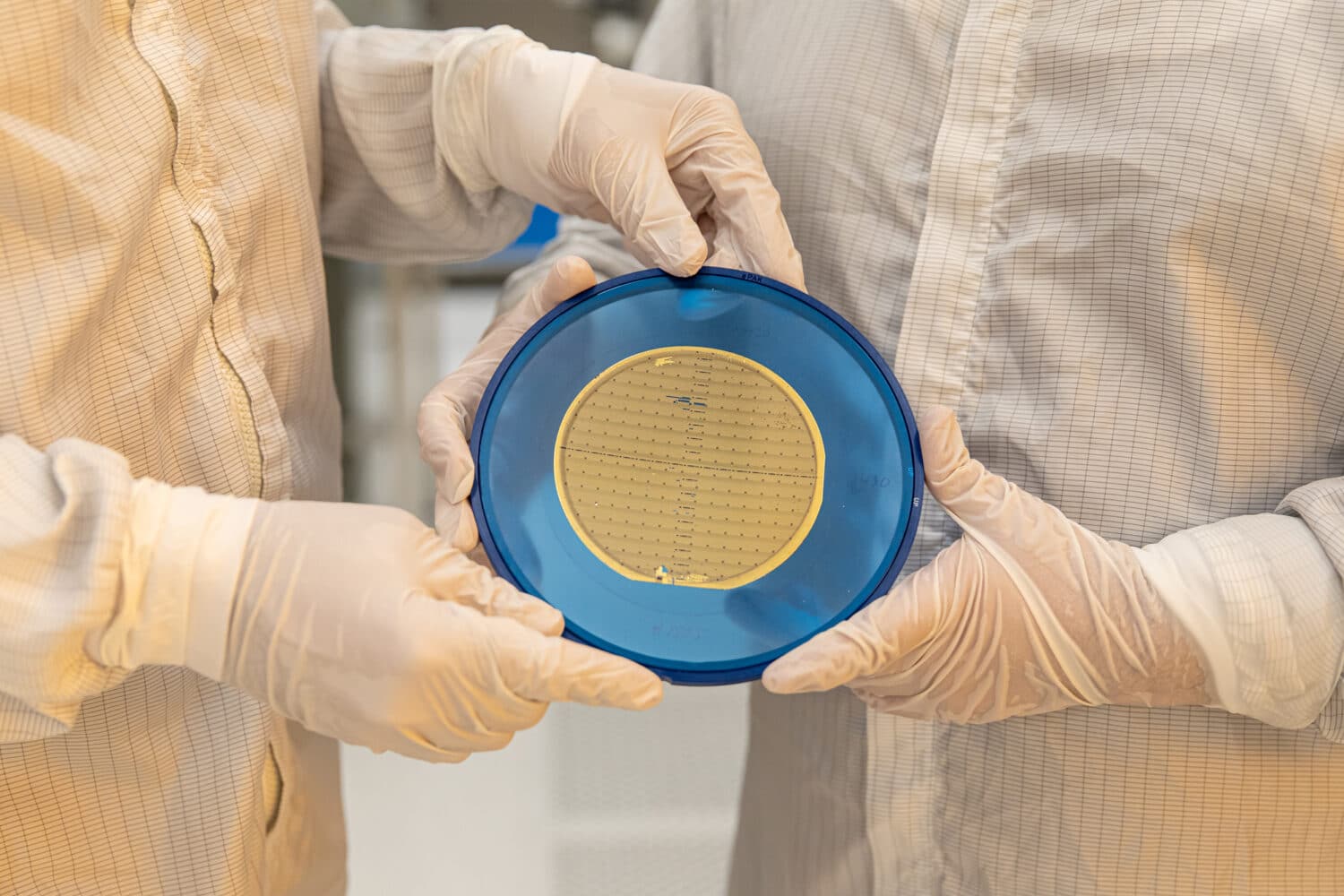
“Our transistors are produced using electron beam and laser lithography. Precision is measured in nanometers and single layers of atoms – this level of accuracy defines the quality of our amplifiers,” says Arsalan Pourkabirian, Head of Semiconductor Devices at Low Noise Factory.

This access allows LNF to fine-tune every step of its transistor fabrication process and iterate quickly. By leveraging this unique opportunity, the company has successfully maintained a competitive edge in the industry.

Highlights and events

The world’s first Arctic weather satellite was launched into orbit in 2024. Now, the Chalmers-based technology used in the satellite’s microwave radiometers will be deployed in Europe’s new weather satellite programme, EPS-Sterna. Image: European Space Agency
2026 03 27
Myfab Chalmers

Chalmers research at the heart of record order for Europe’s new weather satellites

Read more
Event
2026 03 23
Myfab Chalmers , Myfab , Myfab KTH , Myfab Lund , Myfab Uppsala

April 15: Myfab joins SEMICON 2026

Read more
The conceptual image shows how the researchers’ sculpted pattern of tiny hills and valleys – smaller than one millionth of a hair’s thickness – on the substrate (MgO, at the bottom) guides how the atoms in the superconducting material (YBCO, on top) settle. At the interface between the two layers, an electronic landscape allows superconductivity to occur at higher temperatures than previously possible – even when high magnetic fields were are applied. Credit: Chalmers University of Technology / Riccardo Arpaia
2026 03 18
Myfab Chalmers

Superconductor advance could unlock ultra-energy-efficient electronics

Read more
Event a university house - Ångström Laboratory - Myfab Uppsala
2026 03 12
Myfab Chalmers , Myfab , Myfab KTH , Myfab Lund , Myfab Uppsala

June 1-3: Nordic user meeting in Uppsala

Read more
See all highlights