Skip to content

APR Technologies develops core pump technology at Myfab Uppsala

Myfab Uppsala

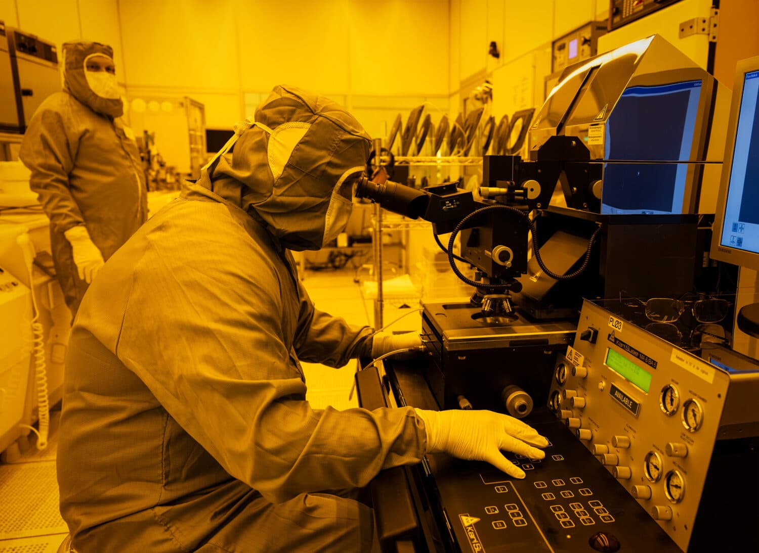
APR Technologies AB, based in Enköping, Sweden, is advancing its core pump technology through cutting-edge microfabrication – an essential yet resource-intensive process.

As the technology is still undergoing development and verification, the company has opted against investing in dedicated fabrication facilities at this stage. Instead, APR leverages access to Myfab. This provides APR with a professionally maintained environment that includes advanced equipment, chemical handling protocols, high cleanliness standards, and specialized processes such as lithography.

“This collaboration allows us to focus our resources on innovation and product development, without the overhead of building and maintaining our own fabrication labs,” says Peter Nilsson (CEO). “It enables us to accelerate R&D, ensure process reliability, and maintain flexibility as our technology matures.”

APR Technologies specializes in advanced thermal management solutions for space and ground-based electronics and battery systems. Their compact, low-power, and vibration-free products use dielectric fluids and electrohydrodynamic (EHD) pumping technology. The company’s portfolio includes both passive and active systems – such as thermal switches, heat exchangers, and fluid loops—designed to optimize performance in demanding applications across space, ICT, and battery sectors.

Highlights and events

The world’s first Arctic weather satellite was launched into orbit in 2024. Now, the Chalmers-based technology used in the satellite’s microwave radiometers will be deployed in Europe’s new weather satellite programme, EPS-Sterna. Image: European Space Agency
2026 03 27
Myfab Chalmers

Chalmers research at the heart of record order for Europe’s new weather satellites

Read more
Event
2026 03 23
Myfab Chalmers , Myfab , Myfab KTH , Myfab Lund , Myfab Uppsala

April 15: Myfab joins SEMICON 2026

Read more
The conceptual image shows how the researchers’ sculpted pattern of tiny hills and valleys – smaller than one millionth of a hair’s thickness – on the substrate (MgO, at the bottom) guides how the atoms in the superconducting material (YBCO, on top) settle. At the interface between the two layers, an electronic landscape allows superconductivity to occur at higher temperatures than previously possible – even when high magnetic fields were are applied. Credit: Chalmers University of Technology / Riccardo Arpaia
2026 03 18
Myfab Chalmers

Superconductor advance could unlock ultra-energy-efficient electronics

Read more
Event a university house - Ångström Laboratory - Myfab Uppsala
2026 03 12
Myfab Chalmers , Myfab , Myfab KTH , Myfab Lund , Myfab Uppsala

June 1-3: Nordic user meeting in Uppsala

Read more
See all highlights