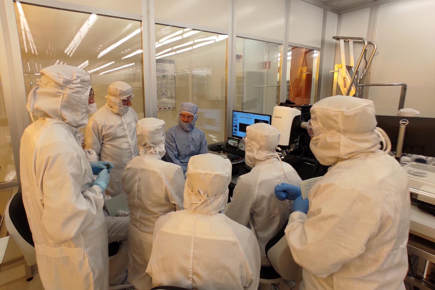
From June 24–26, Myfab Chalmers held a three-day training focused on automated meteorology. Researchers and engineers explored advanced automated characterisation techniques and analysis.
The program began with a lecture on how design and material choices affect fabrication and tool selection. Participants learned about key metrology concepts and how automated systems at Chalmers help ensure wafer quality. A case study showed how metrology helped correct wafer-scale non-uniformities.
Hands-on labs included electrical probing of wafer-wide junction resistance, followed by data analysis using custom scripts. On day two, participants created heatmaps and defect maps, then used automated SEM and optical microscopes to investigate failure modes. They also measured film thickness with an optical profilometer and analyzed the data using statistical tools.
The final day focused on defect inspection in SiN films using a Nikon automated microscope. The course ended with a lecture on broader metrology applications and challenges in data analysis.
This training is part of InfraChip, a European initiative (2024–2027) aiming to build a distributed infrastructure for sustainable semiconductor development. InfraChip connects research communities like ASCENT+, EMERGE, and EnABLES, and promotes innovation in materials and processes. It also invests in talent development through hands-on training—such as the course at Chalmers.
Together, these efforts strengthen Europe’s capacity to innovate in semiconductor technologies, from research to industrial application.