Skip to content

Online traing on high-frequency technologies

datorskärm med teamsmöte

High-frequency technologies like THz electronics, RF-MEMS, photonics, and radio engineering are central to modern innovation. As they evolve rapidly, education is essential to empower more people to drive research, development, and commercialization. Take part in free online training.

Video – INFRACHIP Digital School- CONNECT (Oct 27, 2025)
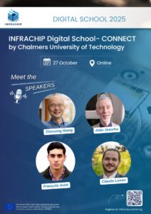
Speakers Zhenxining Wang, Chalmers Aldo Jesorka, Chalmers François Joint, Chalmers Claude Leiner, Joanneum Resea

Speakers:

  • Zhenxing Wang explored 2D materials for THz devices
  • Aldo Jesorka presented RF-MEMS for liquid sensing
  • François Joint shared insights on RF for radio telescopes
  • Claude Leiner discussed photonic system development

A one-day online event on cutting-edge topics including:
• Surface Acoustic Resonance
• RF Engineering
• Advanced Photonics
• THz Range Electronics

This training is part of  InfraChip, a European initiative (2024–2027) aiming to build a distributed infrastructure for sustainable semiconductor development. InfraChip connects research communities like ASCENT+, EMERGE, and EnABLES, and promotes innovation in materials and processes. It also invests in talent development through hands-on training—such as the course at Chalmers. Together, these efforts strengthen Europe’s capacity to innovate in semiconductor technologies, from research to industrial application.

Highlights and events

The world’s first Arctic weather satellite was launched into orbit in 2024. Now, the Chalmers-based technology used in the satellite’s microwave radiometers will be deployed in Europe’s new weather satellite programme, EPS-Sterna. Image: European Space Agency
2026 03 27
Myfab Chalmers

Chalmers research at the heart of record order for Europe’s new weather satellites

Read more
Event
2026 03 23
Myfab Chalmers , Myfab , Myfab KTH , Myfab Lund , Myfab Uppsala

April 15: Myfab joins SEMICON 2026

Read more
The conceptual image shows how the researchers’ sculpted pattern of tiny hills and valleys – smaller than one millionth of a hair’s thickness – on the substrate (MgO, at the bottom) guides how the atoms in the superconducting material (YBCO, on top) settle. At the interface between the two layers, an electronic landscape allows superconductivity to occur at higher temperatures than previously possible – even when high magnetic fields were are applied. Credit: Chalmers University of Technology / Riccardo Arpaia
2026 03 18
Myfab Chalmers

Superconductor advance could unlock ultra-energy-efficient electronics

Read more
Event a university house - Ångström Laboratory - Myfab Uppsala
2026 03 12
Myfab Chalmers , Myfab , Myfab KTH , Myfab Lund , Myfab Uppsala

June 1-3: Nordic user meeting in Uppsala

Read more
See all highlights