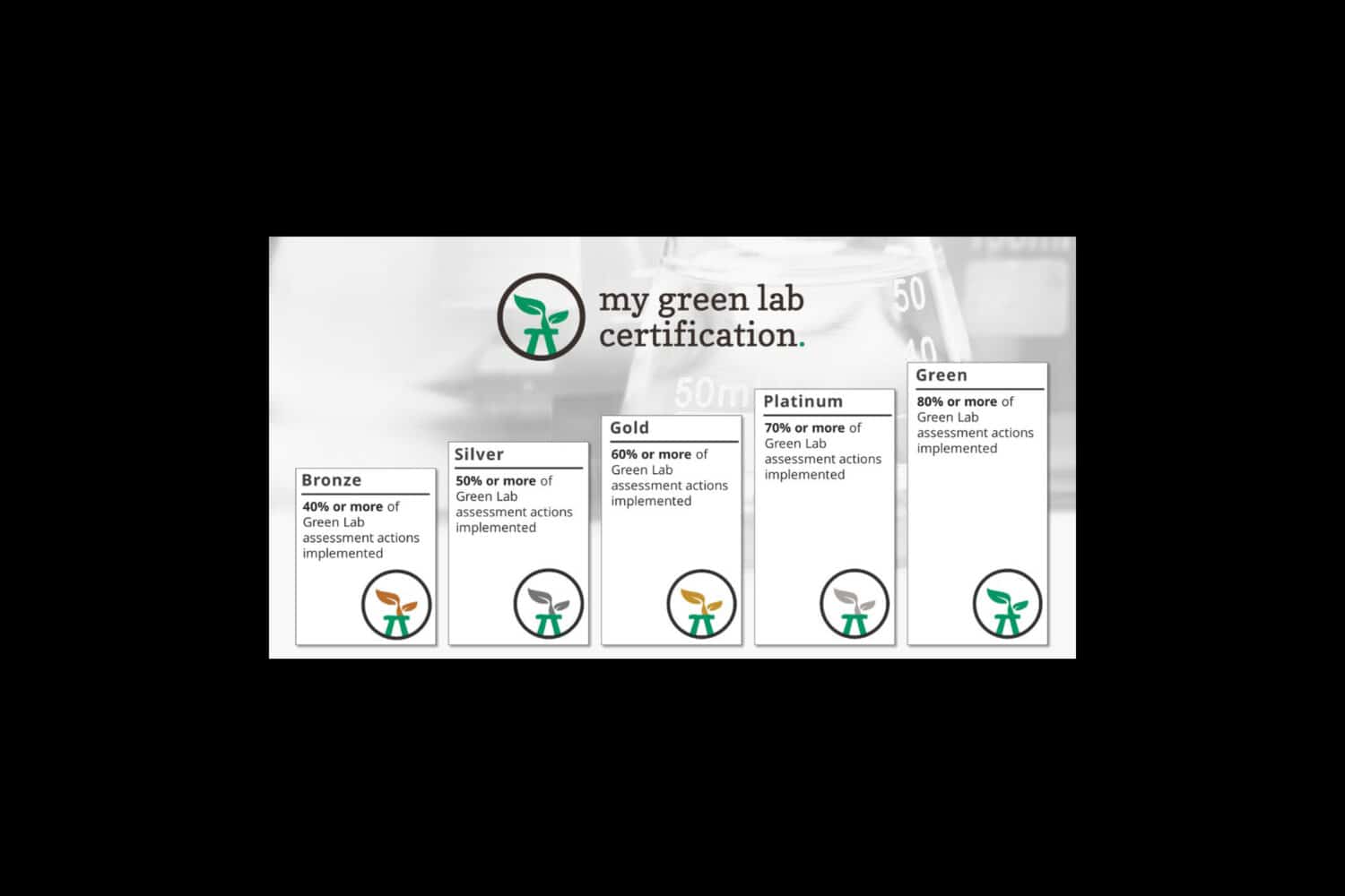
Lund Nano Lab has been awarded Platinum Certification by My Green Lab – one of the highest levels of recognition in the global program for sustainable laboratories. It is the second lab within the Myfab network to receive such a distinction, following Myfab KTH, which is certified according to the ISO 14001 environmental management standard.
The certification is the result of the “Greening Lund Nano Lab” project, initiated by Sarah McKibbin and funded by the Lund University Sustainability Fund. The project focused on optimizing lab routines, reducing unnecessary use of consumables, increasing recycling, and encouraging more sustainable user behavior.
Following a comprehensive sustainability assessment, Lund Nano Lab was awarded Platinum level certification by My Green Lab. This achievement highlights the lab’s strong commitment to improving environmental performance in advanced research environments.
“The team will continue to implement further sustainability measures and actively engage with the user community to raise awareness and promote responsible lab practices,” says Luke Hankin, Head of Lund Nano Lab (Myfab Lund). “Support from Tillväxtverket – the Swedish Agency for Economic and Regional Growth – will help us build on this momentum and ensure that greening the lab remains a long-term priority.”
This recognition strengthens Myfab’s commitment to sustainable research infrastructure and sets a strong example for other labs in the network.