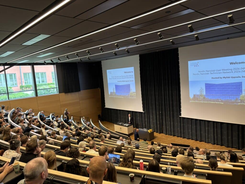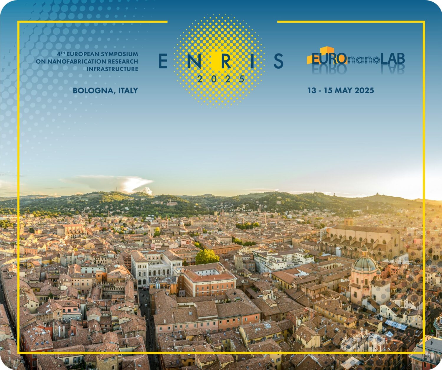
ENRIS (European Symposium on Nanofabrication Research Infrastructure) is a biannual international symposium focused on nanofabrication cleanroom operation, management, and user training. The 4th edition will be held in Bologna.
Time: May 13-15
Venue: CNR (Consiglio Nazionale delle Ricerche)
ENRIS brings together experts and stakeholders in the field to discuss advancements and share knowledge. The conference aims to foster collaboration and innovation in nanofabrication technologies.
ENRIS 2025 is jointly arranged by It-fab, the Italian Network of Nano- and Microfabrication, under the leadership of Stefano Zampolli (Chair of Local Organising Committee) and Thomas Swahn (Chair of Programme Committee).
ENRIS is organised by the European consortium EURONANOLAB (euronanolab.eu).
Myfab has actively contributed to the formation of EuroNanoLab (ENL) through collaboration with its member research infrastructures. ENL consists of over 40 cleanroom-based nanotechnology laboratories across Europe. Inspired by Myfab’s user-fee based open access model, ENL aims to accelerate micro- and nanotechnology research by integrating fragmented facilities into a unified knowledge base. The network supports scientific excellence and provides fast access to results, addressing societal challenges in energy, environment, transport, health, and wellbeing.
Contact
Myfab Director: Thomas Swahn
+46 31 772 46 76, thomas.swahn@chalmers.se