Skip to content

Inauguration – WBG Pilot Line

Picture: WBG Pilot Line

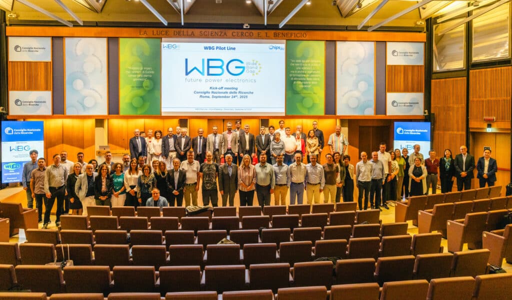
European research institutions and industry partners gathered in Rome for the official kick-off of the Wide Bandgap (WBG) Pilot Line project. Myfab KTH, Lund and Chalmers together with Linköping University will serve as nodes for the development and testing of these technologies.

The WBG Pilot Line project aims to establish a European infrastructure for the development and integration of advanced semiconductor materials and devices, including SiC bipolar, GaN RF, and ultra-wide bandgap technologies. These innovations are expected to significantly enhance the performance and efficiency of power electronics across sectors such as energy, mobility, and telecommunications.

At the event: Peter Modh, Chalmers – Vanya Darakchieva, Lund University – Mikael Östling, KTH

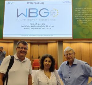
The event marked the beginning of a collaborative effort to develop next-generation power electronics based on wide bandgap semiconductor technologies.

The agenda featured presentations from representatives of the European Commission, national ministries, and leading research organizations such as CNR, Fraunhofer IISB, CEA LETI, and FBK. Swedish partners, including Vanya Darakchieva from Lund University, highlighted Sweden’s role in advancing ultra-wide bandgap semiconductors and device integration.

The project is structured around ten work packages, covering everything from material development and device fabrication to dissemination and training. Myfab’s involvement ensures that Swedish research infrastructure remains at the forefront of European semiconductor innovation.

Highlights and events

The world’s first Arctic weather satellite was launched into orbit in 2024. Now, the Chalmers-based technology used in the satellite’s microwave radiometers will be deployed in Europe’s new weather satellite programme, EPS-Sterna. Image: European Space Agency
2026 03 27
Myfab Chalmers

Chalmers research at the heart of record order for Europe’s new weather satellites

Read more
Event
2026 03 23
Myfab Chalmers , Myfab , Myfab KTH , Myfab Lund , Myfab Uppsala

April 15: Myfab joins SEMICON 2026

Read more
The conceptual image shows how the researchers’ sculpted pattern of tiny hills and valleys – smaller than one millionth of a hair’s thickness – on the substrate (MgO, at the bottom) guides how the atoms in the superconducting material (YBCO, on top) settle. At the interface between the two layers, an electronic landscape allows superconductivity to occur at higher temperatures than previously possible – even when high magnetic fields were are applied. Credit: Chalmers University of Technology / Riccardo Arpaia
2026 03 18
Myfab Chalmers

Superconductor advance could unlock ultra-energy-efficient electronics

Read more
Event a university house - Ångström Laboratory - Myfab Uppsala
2026 03 12
Myfab Chalmers , Myfab , Myfab KTH , Myfab Lund , Myfab Uppsala

June 1-3: Nordic user meeting in Uppsala

Read more
See all highlights