Skip to content

Nordic user meeting: NNTN & NNUM in Uppsala

a university house - Ångström Laboratory - Myfab Uppsala

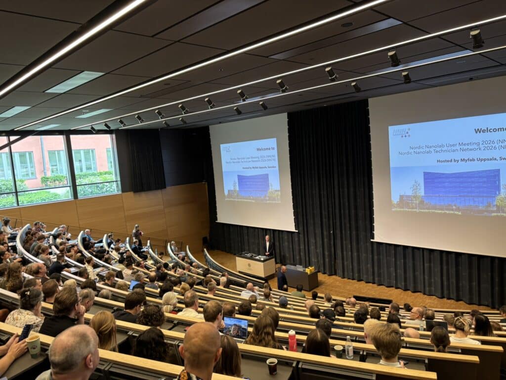
In June, Myfab Uppsala will host user and technician meetings for the Nordic Nanolab Network. Over three days, researchers, students, engineers, and cleanroom technicians from twelve Nordic facilities will meet to share knowledge, develop skills, and build new collaborations through workshops, talks, networking, and guided lab tours.

Nordic Nanolab User Meeting 2026 (NNUM 2026)
The fifth Nordic Nanolab User Meeting.
Time: June 2 – June 3, 2026
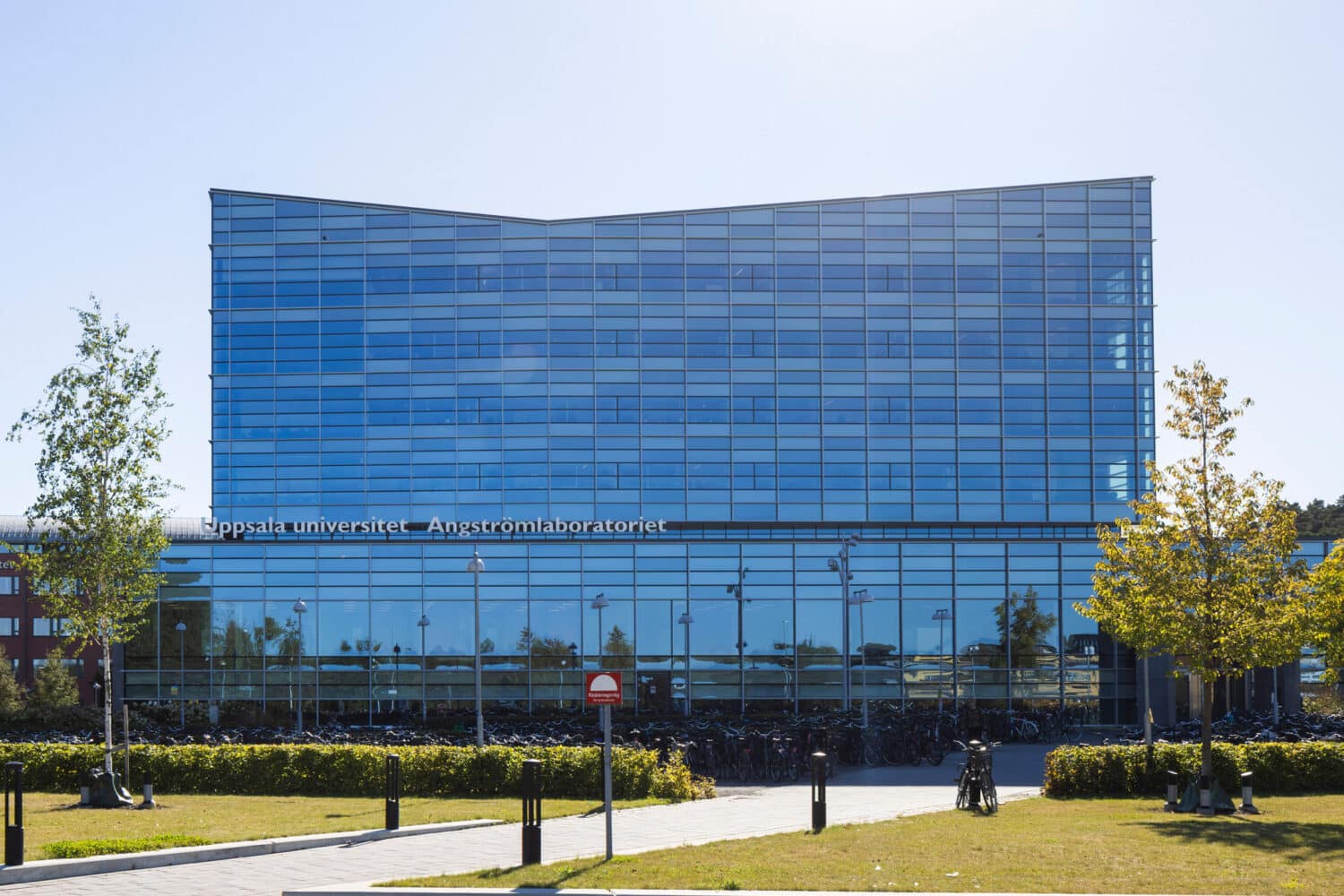
Place:  Ångström Laboratory, Lägerhyddsvägen 1, Uppsala, Sweden

Nordic Nanolab Technician Network 2026 (NNTN 2026):
This event will is for technicians at the NNN member cleanrooms.
Time: June 1 – June 2, 2026
Place: Ångström Laboratory

Both events are organised by the Nordic Nanolab Network, a collaborative network formed by the national research infrastructures for micro- and nanofabrication in the Nordic countries.

Register latest March 15 NNUM & NNTN 2026

The Nordic infrastructures are crucial for advancing technologies that drive progress in medical tech, electronics, materials science, and environmental solutions.

Highlights and events

The conceptual image shows how the researchers’ sculpted pattern of tiny hills and valleys – smaller than one millionth of a hair’s thickness – on the substrate (MgO, at the bottom) guides how the atoms in the superconducting material (YBCO, on top) settle. At the interface between the two layers, an electronic landscape allows superconductivity to occur at higher temperatures than previously possible – even when high magnetic fields were are applied. Credit: Chalmers University of Technology / Riccardo Arpaia
2026 03 18
Myfab Chalmers

Superconductor advance could unlock ultra-energy-efficient electronics

Read more
Illustration of the device concept. A memory chip based on stacked quantum materials. By placing a magnetic layer on top of a topological material, the researchers were able to switch magnetization using very small electrical currents and without applying an external magnetic field. Illustration: Lalit Pandey
2026 03 11
Myfab Chalmers

Quantum materials breakthrough for energy-efficient data processing

Read more
Ove Öhman has been a bridge-builder between academia and the business sector for several decades and has helped strengthen Uppsala’s innovation environment. Photo: Mikael Wallerstedt, Uppsala University
2026 03 10
Myfab Uppsala

Ove Öhman receives prize as a bridge-builder between research and innovation

Read more
A research team at Chalmers University of Technology has developed a new diminutive laser technology that makes it possible to create a miniature biosensor with the laser source and optics integrated onto a one-centimetre semiconductor chip. This enables significantly smaller sensors, paving the way for portable optical technology and for moving certain types of medical sampling from hospitals to the patients’ homes. Illustration: Chalmers/Erik Strandberg
2026 03 10
Myfab Chalmers

Miniature laser technology could bring lab testing into your home

Read more
See all highlights