Skip to content

Highlights

The conceptual image shows how the researchers’ sculpted pattern of tiny hills and valleys – smaller than one millionth of a hair’s thickness – on the substrate (MgO, at the bottom) guides how the atoms in the superconducting material (YBCO, on top) settle. At the interface between the two layers, an electronic landscape allows superconductivity to occur at higher temperatures than previously possible – even when high magnetic fields were are applied. Credit: Chalmers University of Technology / Riccardo Arpaia
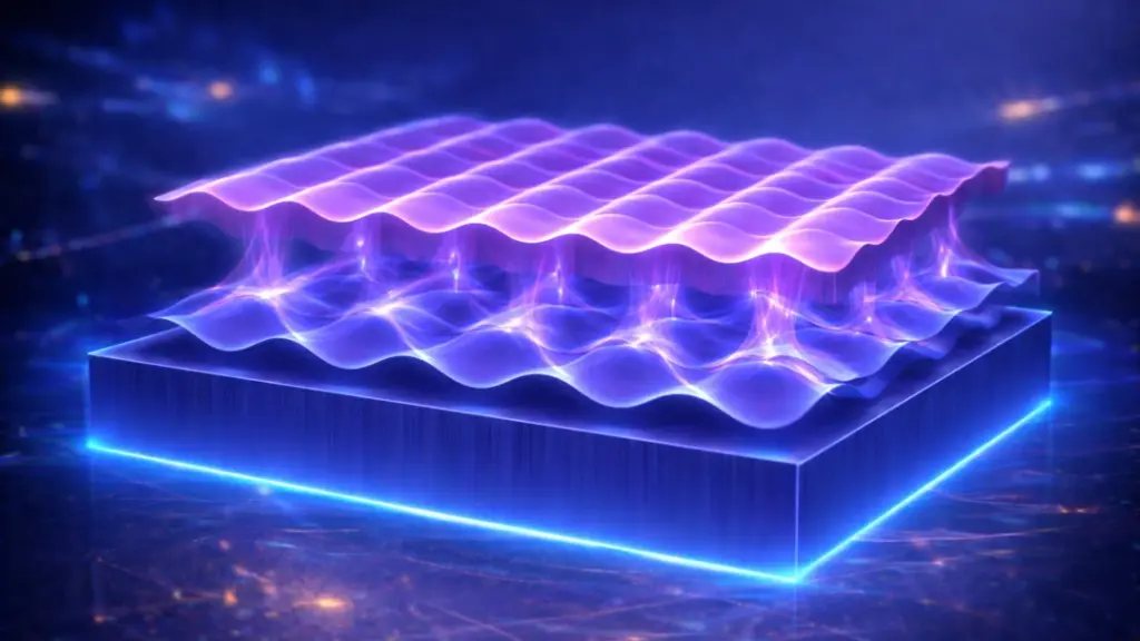
2026 03 18
Myfab Chalmers

Superconductor advance could unlock ultra-energy-efficient electronics

Read more
Event a university house - Ångström Laboratory - Myfab Uppsala
2026 03 12
Myfab Chalmers , Myfab , Myfab KTH , Myfab Lund , Myfab Uppsala

Nordic user meeting: NNTN & NNUM in Uppsala

Read more
Illustration of the device concept. A memory chip based on stacked quantum materials. By placing a magnetic layer on top of a topological material, the researchers were able to switch magnetization using very small electrical currents and without applying an external magnetic field. Illustration: Lalit Pandey
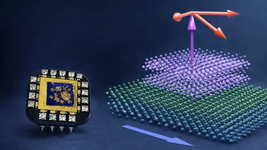
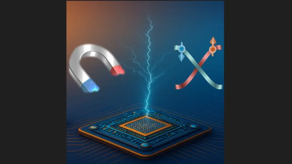
2026 03 11
Myfab Chalmers

Quantum materials breakthrough for energy-efficient data processing

Read more
A research team at Chalmers University of Technology has developed a new diminutive laser technology that makes it possible to create a miniature biosensor with the laser source and optics integrated onto a one-centimetre semiconductor chip. This enables significantly smaller sensors, paving the way for portable optical technology and for moving certain types of medical sampling from hospitals to the patients’ homes. Illustration: Chalmers/Erik Strandberg
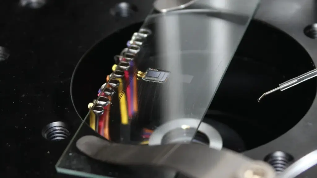
2026 03 10
Myfab Chalmers

Miniature laser technology could bring lab testing into your home

Read more
2026 02 05
Myfab Chalmers

Humidity-resistant hydrogen sensor can improve safety in large-scale clean energy

Read more
2026 01 29
Myfab Chalmers

Novel quantum refrigerator benefits from problematic noise

Read more
AMSwitch proposed an altermagnetic chip that harnesses a new class of quantum magnetic materials called altermagnets, distinguished by their alternating and huge spin-split electronic states. The schematics depict the chip alongside a magnet (left) and a band structure (right) revealing a pronounced spin splitting between the up-spin (red) and down-spin (blue) electronic bands.
2026 01 23
Myfab Chalmers

Major EU funding for new generation of quantum magnetic chips

Read more
2026 01 07
Myfab Chalmers

Chalmers launches excellence program to reach the top in Europe

Read more
2025 12 03
Myfab Chalmers

Nils Engelsen recives Wallenberg Academy Fellow grant

Read more
2025 11 28
Myfab Chalmers , Myfab , Myfab KTH , Myfab Lund , Myfab Uppsala

The Swedish Research Council has awarded Myfab with 27 MSEK additional funding to ensure that the infrastructure can meet the advanced needs of upcoming excellence clusters for ground-breaking technology.

Read more
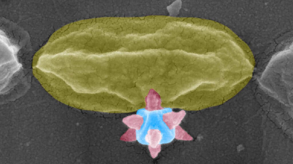
2025 11 27
Myfab Chalmers , Myfab

Nobel Prize-awarded material that puncture and kill bacteria

Read more