The Nordic Nanolab Network is a collaborative network of national research infrastructures for micro- and nanofabrication across the Nordic countries. With 12 cleanrooms in the region, NNN improves access for both academic and industrial users.
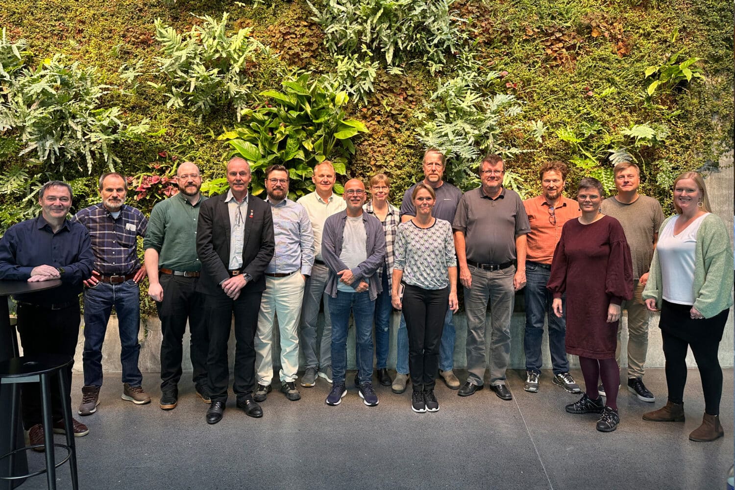
The management meeting was held in Reykjavík, hosted by the University of Iceland and its nanolab and materials science center, led by Unnar Arnalds.
The agenda included a tour of the university’s facilities with briefings on current activities, roundtable discussions, and a visit to the volcanic area just outside Reykjavík.
The network’s key value lies in facilitating the exchange of experiences—both challenges and successes—across areas such as operational and safety-related technical issues, infrastructure development, talent acquisition, and funding and sustainability conditions.
NNN’s infrastructures are crucial for advancing technologies that drive progress in medical tech, electronics, materials science, and environmental solutions – strengthening Europe’s semiconductor ecosystem.